
Page 44 - System on Package_ Miniaturization of the Entire System
P. 44
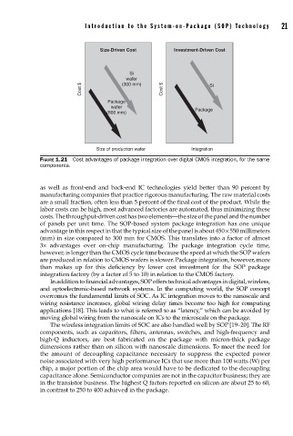
Intr oduction to the System-on-Package (SOP) Technology       21


                                       Size-Driven Cost       Investment-Driven Cost


                                                Si
                                               wafer
                                 Cost $       (300 mm)     Cost $         Si

                                          Package
                                           wafer
                                                                     Package
                                         (600 mm)


                                      Size of production wafer      Integration
                    FIGURE 1.21  Cost advantages of package integration over digital CMOS integration, for the same
                    components.


                    as well as front-end and back-end IC technologies yield better than 90 percent by
                    manufacturing companies that practice rigorous manufacturing. The raw material costs
                    are a small fraction, often less than 5 percent of the final cost of the product. While the
                    labor costs can be high, most advanced factories are automated, thus minimizing these
                    costs. The throughput-driven cost has two elements—the size of the panel and the number
                    of panels per unit time. The SOP-based system package integration has one unique
                    advantage in this respect in that the typical size of the panel is about 450 × 550 millimeters
                    (mm) in size compared to 300 mm for CMOS. This translates into a factor of almost
                    3× advantages over on-chip manufacturing. The package integration cycle time,
                    however, is longer than the CMOS cycle time because the speed at which the SOP wafers
                    are produced in relation to CMOS wafers is slower. Package integration, however, more
                    than makes up for this deficiency by lower cost investment for the SOP package
                    integration factory (by a factor of 5 to 10) in relation to the CMOS factory.
                       In addition to financial advantages, SOP offers technical advantages in digital, wireless,
                    and optoelectronic-based network systems. In the computing world, the SOP concept
                    overcomes the fundamental limits of SOC. As IC integration moves to the nanoscale and
                    wiring resistance increases, global wiring delay times become too high for computing
                    applications [18]. This leads to what is referred to as “latency,” which can be avoided by
                    moving global wiring from the nanoscale on ICs to the microscale on the package.
                       The wireless integration limits of SOC are also handled well by SOP [19–20]. The RF
                    components, such as capacitors, filters, antennas, switches, and high-frequency and
                    high-Q inductors, are best fabricated on the package with micron-thick package
                    dimensions rather than on silicon with nanoscale dimensions. To meet the need for
                    the amount of decoupling capacitance necessary to suppress the expected power
                    noise associated with very high performance ICs that use more than 100 watts (W) per
                    chip, a major portion of the chip area would have to be dedicated to the decoupling
                    capacitance alone. Semiconductor companies are not in the capacitor business; they are
                    in the transistor business. The highest Q factors reported on silicon are about 25 to 60,
                    in contrast to 250 to 400 achieved in the package.