
Page 42 - System on Package_ Miniaturization of the Entire System
P. 42
Intr oduction to the System-on-Package (SOP) Technology 19
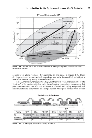
2 nd Law of Electronics by SOP
10 10 10 8
Moore’s law 7
10 9 for ICs 10
10 8 10% System 10 6
Transistors/cm 3 10 7 6 Moore’s law for ICs 90% System Nano 10 5 4 Component density or functional density/cm 3
10
10
System
10 5 MCM, 3D, SIP integration law 2005 SOP 10 3
2010
Micro PRC-2003
10 4 10 2
MILLI
Component density 50
10 3 SMT MCM 10
PTH
1971 1980 1990 2000 2004 2020
FIGURE 1.18 Second law of electronics achieves true package integration combined with the
best of IC integration.
a number of global package developments, as illustrated in Figure 1.19. These
developments can be summarized as package size reductions enabled by I/O pitch
reductions enabled by wiring and via dimensions.
In the SOP concept, “the system package, not the bulky board, is the system.” While
“systems” of the past consisted of bulky boxes housing hundreds of components that
performed one task, the SOP concept consists of small and highly integrated and
microminiaturized components in a single system package or module with system
Evolution of IC Packages
SoP
SIP
Family QFP BGA FC-BGA DCA Non-TSV TSV SoP
IC Wire bond Wire bond Solder ball ---- WB, FC TSV Flip chip
Package Leadframe Substrate Substrate Thin-film Substrate Substrate Substrate
Si efficiency 30 50 75 100 >100 >100 >100
FIGURE 1.19 IC packaging evolution. (Courtesy: Infi neon)