
Page 49 - System on Package_ Miniaturization of the Entire System
P. 49
26 Cha pte r O n e
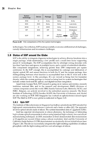
System Device Package System End system
technology board
SOB IC Bulky Bulky Bulky
SOC SOC Bulky Bulky Less bulky
MCM IC MCM Bulky Miniaturized
SIP SOC SIP Bulky Miniaturized
Highly
System miniaturized
SOP SOC SIP
integration nano-micro
system
FIGURE 1.24 Size comparisons of the fi ve system technologies.
technologies. Nevertheless, SOP must successfully overcome a different set of challenges,
namely infrastructure and investment challenges.
1.8 Status of SOP around the Globe
SOP is the ability to integrate disparate technologies to achieve diverse functions into a
single package, while maintaining a low profile and a small form factor supporting
mixed IC technologies. The SOP accomplishes this by ultrahigh wiring densities with
less than 5-μm lines and spaces, in multiple layers, and a variety of embedded ultrathin-
film component integrations, achieving greater than 2500 components per square
centimeter. In the SOP concept, this is accomplished by codesign and fabrication of
digital, optical, RF, and sensor functions in both the IC and the system package, thus
distinguishing between what function is accomplished best at the IC level and at the
system package level. In this paradigm, ICs are viewed as being best for transistor
density, while the system package is viewed as being best for system technologies that
include certain front-end RF, optical, and digital-function integration.
Apart from Georgia Tech, SOP research is going on in various universities, research
institutes, national labs, and in the research and development (R&D) divisions of
various companies across the world. IBM; Sandia National Labs; Motorola; NCSU; and
IMEC, Belgium, are actively involved in the embedded passives research. The Royal
Institute of Technology (KTH) Sweden, KAIST, the University of Arkansas, and Alcatel
are also working on SOP. IME Singapore has worked on optoelectronics mixed-signal
SOP. The R&D in SOP is now global as indicated in Figure 1.25.
1.8.1 Opto SOP
The Institute of Microelectronics in Singapore has built an optoelectronic SOP intended for
high-speed communications between a network and a home or office [42]. The approach
involves optical circuits made of silicon. The system transmitted data at 1 gigahertz (GHz).
Intel has reported developments in silicon photonics, the technique of fabricating
high-volume optical components in silicon using standard high-volume, low-cost silicon
manufacturing techniques. In 2005, researchers at Intel demonstrated data transmission
at 10 gigabits per second (Gbps) using a silicon modulator. Intel and the University of
California Santa Barbara (UCSB) demonstrated an electrically driven hybrid silicon laser
(Figure 1.26). This device successfully integrates the light-emitting capabilities of indium
phosphide with the light-routing and low-cost advantages of silicon.