
Page 99 - System on Package_ Miniaturization of the Entire System
P. 99
Intr oduction to System-on-Chip (SOC) 75
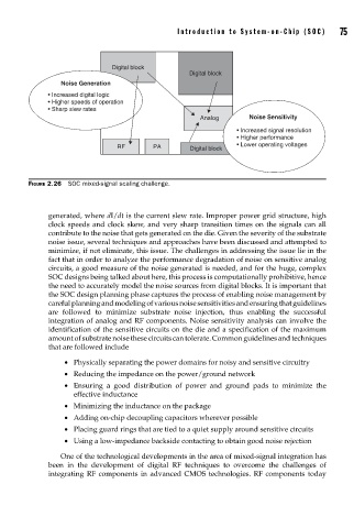
Digital block
Digital block
Noise Generation
• Increased digital logic
• Higher speeds of operation
• Sharp slew rates
Analog Noise Sensitivity
• Increased signal resolution
• Higher performance
RF PA Digital block • Lower operating voltages
FIGURE 2.26 SOC mixed-signal scaling challenge.
generated, where dI/dt is the current slew rate. Improper power grid structure, high
clock speeds and clock skew, and very sharp transition times on the signals can all
contribute to the noise that gets generated on the die. Given the severity of the substrate
noise issue, several techniques and approaches have been discussed and attempted to
minimize, if not eliminate, this issue. The challenges in addressing the issue lie in the
fact that in order to analyze the performance degradation of noise on sensitive analog
circuits, a good measure of the noise generated is needed, and for the huge, complex
SOC designs being talked about here, this process is computationally prohibitive, hence
the need to accurately model the noise sources from digital blocks. It is important that
the SOC design planning phase captures the process of enabling noise management by
careful planning and modeling of various noise sensitivities and ensuring that guidelines
are followed to minimize substrate noise injection, thus enabling the successful
integration of analog and RF components. Noise sensitivity analysis can involve the
identification of the sensitive circuits on the die and a specification of the maximum
amount of substrate noise these circuits can tolerate. Common guidelines and techniques
that are followed include
• Physically separating the power domains for noisy and sensitive circuitry
• Reducing the impedance on the power/ground network
• Ensuring a good distribution of power and ground pads to minimize the
effective inductance
• Minimizing the inductance on the package
• Adding on-chip decoupling capacitors wherever possible
• Placing guard rings that are tied to a quiet supply around sensitive circuits
• Using a low-impedance backside contacting to obtain good noise rejection
One of the technological developments in the area of mixed-signal integration has
been in the development of digital RF techniques to overcome the challenges of
integrating RF components in advanced CMOS technologies. RF components today