
Page 97 - System on Package_ Miniaturization of the Entire System
P. 97
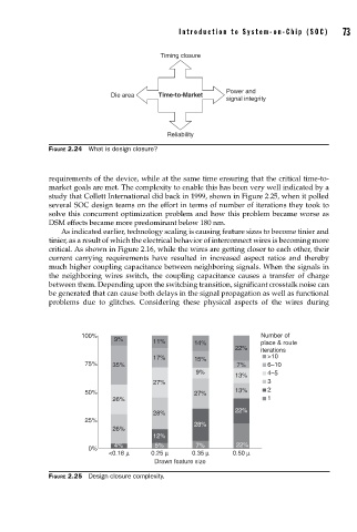
Intr oduction to System-on-Chip (SOC)     73


                                                 Timing closure


                                                                  Power and
                                    Die area     Time-to-Market
                                                                  signal integrity


                                                   Reliability
                    FIGURE 2.24  What is design closure?


                    requirements of the device, while at the same time ensuring that the critical time-to-
                    market goals are met. The complexity to enable this has been very well indicated by a
                    study that Collett International did back in 1999, shown in Figure 2.25, when it polled
                    several SOC design teams on the effort in terms of number of iterations they took to
                    solve this concurrent optimization problem and how this problem became worse as
                    DSM effects became more predominant below 180 nm.
                       As indicated earlier, technology scaling is causing feature sizes to become tinier and
                    tinier, as a result of which the electrical behavior of interconnect wires is becoming more
                    critical. As shown in Figure 2.16, while the wires are getting closer to each other, their
                    current carrying requirements have resulted in increased aspect ratios and thereby
                    much higher coupling capacitance between neighboring signals. When the signals in
                    the neighboring wires switch, the coupling capacitance causes a transfer of charge
                    between them. Depending upon the switching transition, significant crosstalk noise can
                    be generated that can cause both delays in the signal propagation as well as functional
                    problems due to glitches. Considering these physical aspects of the wires during


                             100%                                          Number of
                                     9%        11%        14%              place & route
                                                                    22%    iterations
                                                                             >10
                                                                             >10
                                               17%        15%                >10
                              75%    35%                             7%      6- 6- 6–10
                                                          9%                 4- 4- 4–5
                                                                    13%
                                               27%                           3 3 3
                              50%                         27%       13%      2 2 2
                               50
                                     26%                                     1 1 1
                                                                    22%
                                               28%
                              25%
                                                          28%
                                     26%
                                               12%
                                                          7%
                                     4%         5%        7%         22%
                              0%
                              0%
                                               0.25μ
                                    <0.18μ
                                    <0.18      0.25      0.35 μ     0.50 μ
                                                                    0.50
                                                Drawn feature size
                                                 D
                    FIGURE 2.25  Design closure complexity.