
Page 93 - System on Package_ Miniaturization of the Entire System
P. 93
Intr oduction to System-on-Chip (SOC) 69
• Time-to-market • Higher parastics
• Multi-million gates • Interconnect delay
• IP/component reuse • Higher cross-coupling
• Divide & conquer • Power
• Large design database sizes • Electro-migration
• High performance • IR drop
• High density • Package careabouts
Abstraction Accuracy
FIGURE 2.21 SOC versus technology challenges.
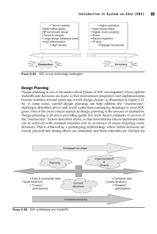
Design Planning
Design planning is one of the most critical phases of SOC development where upfront
tradeoffs and decisions are made so that downstream integration and implementation
become seamless toward achieving overall design closure, as illustrated in Figure 2.22.
So, in some sense, careful design planning can help address the “macroscopic”
challenges described above and avoid costly time-consuming iterations to meet SOC
goals. One of the most critical aspects in design planning is the process of estimation.
Design planning is all about providing quick, but fairly decent estimates of several of
the “microscopic” factors described above, so that downstream silicon implementation
can be achieved with minimal surprises and an avoidance of issues requiring costly
iterations. This is achieved by a prototyping methodology where initial decisions are
forced, physical and timing effects are estimated, and these estimates are checked for
Increased run-times
Implementation
Planning &
Closure
• Early & incomplete data • Complete data
• Quick iterations Commit • Costly iterations
• “Coarse’’ • “Detailed’’
decisions
optimizations optimizations
Increased accuracy
FIGURE 2.22 SOC prototyping and tradeoffs.