
Page 89 - System on Package_ Miniaturization of the Entire System
P. 89
Intr oduction to System-on-Chip (SOC) 65
cells, design tools need to handle optimization techniques to minimize leakage power
by the appropriate usage of cells that have a high V . Typically, the cell libraries that
t
support the multi-V optimization have both fast cells with lower V thresholds (but
t t
higher leakage) and slow cells with higher V thresholds (and hence a smaller leakage
t
component). One approach commonly adopted during design to reduce leakage power
is to deploy the fast cells during the initial logic synthesis, and then swap in the low-
leakage cells during subsequent timing optimization on circuit paths that can use these
low-leakage (but slower in performance) cells without impacting the timing. While
such power optimizations are done, it is very important to also understand the
implications to the chip die area (cost) and yield in terms of sensitivity to process
variation. As silicon technology scales down, the gate oxide thickness also goes down,
and as a result, the oxide layer fails to act as a perfect insulator and leakage current
flows through it. This can be overcome by the use of high-dielectric-constant oxides,
and as a result of this thick oxide, the leakage current is minimized. In addition to
leakage power, the on-chip power density trend is on an exponential rise, as can be seen
2
with the Pentium example: the P-4 had a power density of 46 W/cm , which is seven
times that of the Intel 486. Several techniques for reducing switching power have been
considered in the recent past. Reducing activity, capacitance, and supply voltage are
some of the commonly known methods. Design methodologies such as clock gating,
power gating, power-aware physical design, and voltage scaling have been deployed to
tackle the SOC power efficiency issues for sensitive handheld applications such as
wireless mobile phones, PDAs, and personal multimedia players.
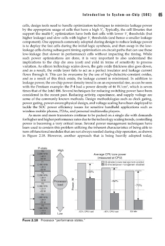
As more and more transistors continue to be packed on a single die with demands
for higher and higher performance rates due to the technology scaling trends, controlling
power is becoming a very critical issue. Several power management techniques have
been used to contain this problem utilizing the inherent characteristics of being able to
turn off functional modules that are not always needed during chip operation, as shown
in Figure 2.18. However, another approach that is being heavily adopted today,
P-state
P0 High
2,600 MHz Average CPU core power
1.40 V
−95 W (measured at CPU)
P1 OS-directed power management–enabled
2,400 MHz OS-directed power management–disabled
1.35 V
−90 W
P2 −33%
2,200 MHz
1.30 V
−76 W
Processor −62%
P3 load Power, W
2,000 MHz −75%
1.25 V
−65 W
P4
1,800 MHz
1.20 V
−55 W
P5
1,000 MHz
1.10 V −62% CPU load −40% CPU load OS idle
−32 W Low
FIGURE 2.18 Processor “performance states.”