
Page 91 - System on Package_ Miniaturization of the Entire System
P. 91
Intr oduction to System-on-Chip (SOC) 67
additional parasitics. This is beginning to be called “yield-driven-layout” in the industry
today. Another major cause of yield concern on the chip are the “via” structures added
to connect adjacent metal interconnects. Thermally induced stress can impact both the
copper interconnects and the low-K materials used in today’s process technology given
that the dielectric has a large thermal expansion coefficient and poor adhesion. This can
cause voids below the via structures and result in poor reliability of the circuit. Layout
designers need to take care of this yield issue during physical design. This is typically
done by optimizing the interconnect routing to minimize vias as much as possible by
ensuring straighter routes, and where vias are added, to insert redundant vias in the
layout so as to improve the reliability of the design.
In contrast to the exciting growth opportunities and enablers toward integrating
and building complex SOC devices with advanced process technology, and the several
huge challenges outlined above, the availability of design engineering talent to support
the creation of such complex SOCs has not increased. This has resulted in a huge design
productivity gap that needs to be addressed.
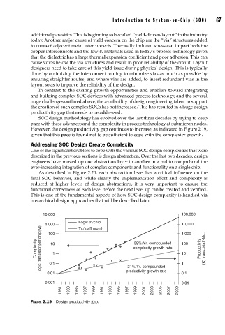
SOC design methodology has evolved over the last three decades by trying to keep
pace with these advances and the complexity in process technology at submicron nodes.
However, the design productivity gap continues to increase, as indicated in Figure 2.19,
given that this pace is found not to be sufficient to cope with the complexity growth.
Addressing SOC Design Create Complexity
One of the significant enablers to cope with the various SOC design complexities that were
described in the previous sections is design abstraction. Over the last two decades, design
engineers have moved up one abstraction layer to another in a bid to comprehend the
ever-increasing integration of complex components and functionality on a single chip.
As described in Figure 2.20, each abstraction level has a critical influence on the
final SOC behavior, and while clearly the implementation effort and complexity is
reduced at higher levels of design abstractions, it is very important to ensure the
functional correctness of each level before the next level up can be created and verified.
This is one of the fundamental aspects of how SOC design complexity is handled via
hierarchical design approaches that will be described later.
10,000 100,000
Logic tr./chip
1,000 Tr./staff month 10,000
1,000
100
Complexity logic transistor per chip(M) 10 1 x x complexity growth rate 100 Productivity (K) trans./staff-Mo.
58%/Yr. compounded
10
0.1
21%/Yr. compounded
0.01 x x x x x x productivity growth rate 1 0.1
0.001 0.01
1981 1983 1985 1987 1989 1991 1993 1995 1997 1999 2001 2003 2005 2007 2009
FIGURE 2.19 Design productivity gap.