
Page 88 - System on Package_ Miniaturization of the Entire System
P. 88
64 Cha pte r T w o
caused lower noise margins. In addition, due to huge SOC die sizes, the high speed of
operation running into gigahertz, and the shrinking of metal layers has caused severe
on-chip IR drop issues. IR drops on the power and ground distribution network can
severely impact chip performance, including the clock signals. Excessive IR drop on the
power grid can cause timing failures in the circuits that designers have to analyze and
comprehend. It has been found that a 10 percent voltage drop in a 180-nm design can
increase propagation gate delays by up to 8 percent [38].
Hunger for MIPS to fuel the ever-growing demand from applications discussed
earlier has pushed up clock rates higher and higher, resulting in several new applications
requiring design and circuit-level innovations. This is also the result of the fact that the
move to a new process node does not necessarily offer significant performance lift. As
the clock frequency increases, the timing margins required for the circuits to operate
dependably across process variations decrease. Increased speed and faster transition
rates on-chip require a more comprehensive handling of issues such as crosstalk and
ground bounce than needed for prior process nodes. Simulation and analysis tools, for
example, need to handle timing, signal integrity, and issues such as electromagnetic
interference (EMI).
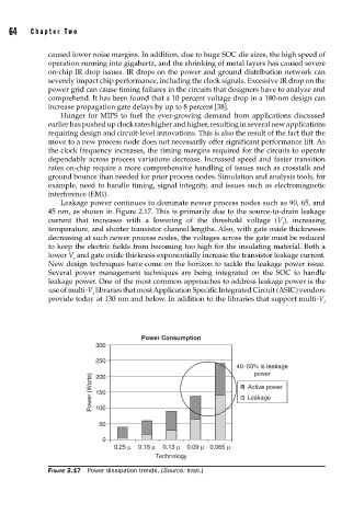
Leakage power continues to dominate newer process nodes such as 90, 65, and
45 nm, as shown in Figure 2.17. This is primarily due to the source-to-drain leakage
current that increases with a lowering of the threshold voltage (V ), increasing
t
temperature, and shorter transistor channel lengths. Also, with gate oxide thicknesses
decreasing at such newer process nodes, the voltages across the gate must be reduced
to keep the electric fields from becoming too high for the insulating material. Both a
lower V and gate oxide thickness exponentially increase the transistor leakage current.
t
New design techniques have come on the horizon to tackle the leakage power issue.
Several power management techniques are being integrated on the SOC to handle
leakage power. One of the most common approaches to address leakage power is the
use of multi-V libraries that most Application Specific Integrated Circuit (ASIC) vendors
t
provide today at 130 nm and below. In addition to the libraries that support multi-V
t
Power Consumption
300
250
40–50% is leakage
power
Power (Watts) 150 Active power
200
Leakage
100
50
0
0.25 μ 0.18 μ 0.13 μ 0.09 μ 0.065 μ
Technology
FIGURE 2.17 Power dissipation trends. (Source: Intel.)