
Page 87 - System on Package_ Miniaturization of the Entire System
P. 87
Intr oduction to System-on-Chip (SOC) 63
the host-side PC-based software used for application development. The SOC verification
needs to ensure that these two software components interface and interact with the
SOC hardware to provide the desired system functionality.
Design for Test
Given that the SOC technology roadmap is moving feverishly toward smaller silicon
feature sizes, the use of newer physical processing methods involving interconnect
materials like copper and low-K dielectric, and the integration and reuse of complex IP
and memory from various sources, it is becoming increasingly important to ensure the
quality and reliability of the silicon used. At the same time the cost involved in measuring
these quality levels needs to also come down to reduce the overall SOC cost. It is
important that the right set of vectors are generated and applied to not just ensure the
ease of detecting manufacturing defects but also to ensure a reduction in the overall test
time. The process of integrating features or logic to enable this is called “design for
test.” While the use of built-in self-test (BIST) techniques for memories have been in
use, increasingly designers are adopting BIST techniques to test logic as well, so as to
achieve higher quality at a lower cost.
Technology Scaling
Process technology is linearly shrinking at approximately 70 percent per generation.
This enables the implemention of a logic function in half the die area compared to the
previous technology node, hence lowering the cost.
While every advanced process technology node provides the 70 percent linear
shrink, the bond pad pitch (for wire-bond packaging) and bump pitch (for flip-chip
packaging) have not scaled accordingly. In addition, I/Os and analog components do
not shrink as much as the standard logic. These factors need to be taken into consideration
when assessing the cost benefit of moving to a new technology node.
Every new process node comes with an increased reticle cost and increased
fabrication cycle time. The wafer manufacturing cost depends on several factors such as
the cost of capital involved in the procurement of steppers and scanners and the cost of
the process material and fabrication facilities. Wafer throughput also impacts the
manufacturing cost, and this throughput is directly dependent on the number and size
of the “steps” printed on the wafer. Typically, a 130-nm mask set can cost around
US$750,000, while the 90-nm mask set costs over 1 million U.S. dollars.
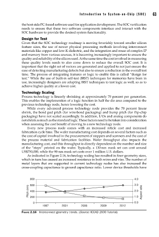
As indicated in Figure 2.16, technology scaling has resulted in finer geometry sizes,
which in turn has caused an increased resistance in both wires and vias. The number of
metal layers that are supported in current technology nodes has also increased the
cross-coupling capacitance to ground capacitance ratio. Lower device thresholds have
800 4.0
3.0
Pitch (nm) 600 2.0 Aspect ratio
400
1.0
200
0 0.0
1997 2001 2006 2009 2012
FIGURE 2.16 Interconnect geometry trends. (Source: ICCAD 2000 Tutorial)