
Page 352 - Sami Franssila Introduction to Microfabrication
P. 352
Tools for CVD and Epitaxy 331
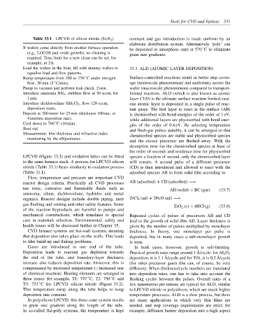
Table 33.1 LPCVD of silicon nitride (Si 3 N 4 ) constant and gas introduction is made uniform by an
elaborate distribution system. Alternatively ‘poly’ can
If wafers come directly from another furnace operation be deposited in amorphous state at 570 C to eliminate
◦
(e.g., LOCOS pad oxide growth), no cleaning is grain size gradients.
required. Time limit for a new clean can be set, for
example, at 2 h.
Load the wafers in the boat, fill with dummy wafers to 33.3 ALD (ATOMIC LAYER DEPOSITION)
equalize load and flow patterns.
◦
Ramp temperature from 500 to 750 C under nitrogen Surface-controlled reactions result in better step cover-
flow, 50 min (5 C/min). age (microscale phenomenon) and uniformity across the
◦
Pump to vacuum and perform leak check, 2 min. wafer (macroscale phenomenon) compared to transport-
Introduce ammonia NH 3 , stabilize flow at 30 sccm, for limited reactions. ALD (which is also known as atomic
1 min. layer CVD) is the ultimate surface-reaction limited case:
Introduce dichlorosilane SiH 2 Cl 2 , flow 120 sccm, one atomic layer is deposited in a single pulse of reac-
deposition starts. tant gases. The first layer to react at the surface (AB)
Deposit at 300 mtorr for 25 min (thickness 100 nm, or is chemisorbed with bond energies of the order of 1 eV,
4 nm/min deposition rate). while additional layers are physisorbed with bond ener-
◦
Cool down to 700 C (10 min). gies of the order of 0.4 eV. By selecting temperature
Boat out. and flush-gas pulses suitably, it can be arranged so that
Measurement: film thickness and refractive index chemisorbed species are stable and physisorbed species
monitoring by the ellipsometer.
and the excess precursor are flushed away. With the
desorption time for the chemisorbed species at least of
the order of seconds and residence time for physisorbed
LPCVD (Figure 33.2) and oxidation tubes can be fitted species a fraction of second, only the chemisorbed layer
to the same furnace stack. A process for LPCVD silicon will remain. A second pulse of a different precursor
nitride (Table 33.1) bears similarity to oxidation process (CD) is then introduced and allowed to react with the
(Table 31.1). adsorbed species AB to form solid film according to
Flow, temperature and pressure are important CVD
reactor design criteria. Practically all CVD processes AB (adsorbed) + CD (adsorbed) −→
use toxic, corrosive and flammable fluids such as AD (solid) + BC (gas) (33.7)
ammonia, silane, dichlorosilane, hydrides and metal
organics. Reactor designs include double piping, inert ZrCl 4 (ad) + 2H 2 O (ad) −→
gas flushing and venting and other safety features. Some ZrO 2 (s) + 4HCl (g) (33.8)
of the reaction byproducts are harmful to pumps and
mechanical constructions, which translates to special Repeated cycles of pulses of precursors AB and CD
care in materials selection. Environmental, safety and lead to the growth of solid film AD. Layer thickness is
health issues will be discussed further in Chapter 35. given by the number of pulses multiplied by monolayer
CVD furnace systems are hot-wall systems, meaning thickness. In theory, one monolayer per pulse is
that deposition also takes place on the walls. This leads deposited, but in many cases a sub-monolayer growth
to film build-up and flaking problems. is seen.
Gases are introduced in one end of the tube. In both cases, however, growth is self-limiting.
Deposition leads to reactant gas depletion towards Practical growth rates range around 1 ˚ A/cycle: for Al 2 O 3
the end of the tube, and boundary-layer thickness deposition, it is 1.1 ˚ A/cycle and for TiN, it is 0.2 ˚ A/cycle
increase also reduces deposition rate. However, this is (for other precursor gases this can, of course, be very
compensated by increased temperature (=increased rate different). When thickness/cycle numbers are translated
of chemical reaction). Heating elements are arranged in into deposition rates, one has to take into account the
◦
◦
three zones: for example, T1: 747 C, T2: 750 C and flushing cycles between the pulses. Overall rates of a
T3: 753 C for LPCVD silicon nitride (Figure 33.2). few nanometres per minute are typical for ALD, similar
◦
This temperature ramp along the tube helps to keep to LPCVD nitride or polysilicon, which are much higher
deposition rate constant. temperature processes. ALD is a slow process, but there
In polysilicon LPCVD, this three-zone system results are many applications in which very thin films are
in grain size gradient along the length of the tube. needed, and step coverage requirements are strict: for
In so-called flat-poly systems, the temperature is kept example, diffusion barrier deposition into a high aspect