
Page 356 - Sami Franssila Introduction to Microfabrication
P. 356
Tools for CVD and Epitaxy 335
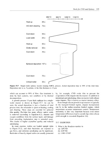
850°C 950°C 1050°C 1150°C
Heat up 26 s
HCl etch cleaning 73 s
Cool down 53 s
Load wafer 25 s
Heat up 55 s
Oxide removal 50 s
Cool down 45 s
Epitaxial deposition 157 s
Cool down 72 s
Unload wafer 32 s
Figure 33.7 Single-wafer epitaxy reactor running SiHCl 3 process. Actual deposition time is 30% of the total time.
Deposition rate is ca. 5 µm/min, or the film thickness is 13 µm
which can account to 99% of flow. Gas treatment is by, for example, CVD oxide film to prevent the
done by burn systems, wet scrubbers or by thermal evaporation of the dopant into the reactor. In addition to
decomposition. intentional and autodoping, films on reactor walls release
A growth process 13 µm thick epilayer in a single- some dopants. This is known as reactor memory effect.
wafer reactor is shown in Figure 33.7. As can be Even though silicon growth in epi reactors is typically
seen, the actual deposition is just a fraction of total in the transport-limited regime, dopant incorporation
process time; the remainder is spent on heating, cooling can be in the surface-reaction limited regime, which
and cleaning. These steps are essential for epitaxial necessitates accurate temperature control. Temperature
film quality. Pre-bake has many effects: native oxide uniformity is also very important because even minor
is removed (according to Equation 6.2), dopants and temperature differences lead to crystal slips when silicon
oxygen outdiffuse from the surface layer, and damage yield strength is exceeded (Equation 4.8).
from preceding implantation step is annealed away.
This results in higher crystalline quality and reduced 33.7 EXERCISES
autodoping.
In some reactors, wafers are loaded upright (akin 1. What is the Knudsen number in
to Figure 33.2), and their backsides are exposed to (a) APCVD
gas flows, and substrate autodoping can be significant. (b) LPCVD
Backsides of heavily doped wafers are usually protected (c) UHV-CVD?