
Page 192 - MEMS Mechanical Sensors
P. 192
8.2 Micromachined Accelerometer 181
8.2.2.1 Piezoresistive Accelerometers
The first micromachined, batch-fabricated accelerometer was reported by Roylance
and Angell [1] at Stanford University in 1979. It used a bulk-micromachined sensing
element consisting of a central silicon wafer that forms the proof mass and a cantile-
ver as its suspension system. The silicon wafer is bonded between two glass wafers
into which cavities are etched to allow the mass to move as a response to accelera-
tion. The glass wafers also protect the proof mass and act as a shock stopper. The
motion of the proof mass was detected with piezoresistors, which were fabricated
by implanting Boron directly in the beams of the silicon suspension system of the
proof mass. In general, early devices tended to use a piezoresistive position measure-
ment interface, as these are easy to fabricate in silicon and the read-out circuit is
relatively simple; they provide a low-impedance output signal and a conventional
resistive bridge circuit can be used. Furthermore, early piezoresistive accelerome-
ters were directly based on the expertise gained through the development of
micromachined pressure sensors. A serious drawback, however, is that the output
signal tends to have a strong temperature dependency because the piezoresistors
inherently produce thermal noise and the output signal is relatively small [11]. Typi-
cal performance figures for these devices show a sensitivity of 1 to 3 mV/g, 5g to 50g
dynamic range, and an uncompensated temperature coefficient of 0.2%/C. Exam-
ples of early devices are described in [12–14]. They typically consist of a multiwafer
assembly with the central wafer comprising the bulk-micromachined proof mass
and suspension system and either silicon or Pyrex glass wafers on top and bottom to
provide over-range protection and near critical damping due to squeeze film effects.
The disadvantages of piezoresistive signal pick-off can be partially overcome by
integrating the read-out electronics on the same chip. A good example is the acceler-
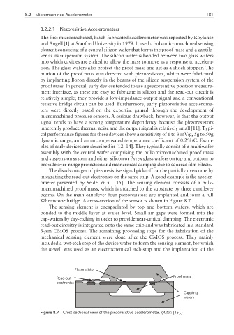
ometer presented by Seidel et al. [15]. The sensing element consists of a bulk-
micromachined proof mass, which is attached to the substrate by three cantilever
beams. On the main cantilever four piezoresistors are implanted and form a full
Wheatstone bridge. A cross-section of the sensor is shown in Figure 8.7.
The sensing element is encapsulated by top and bottom wafers, which are
bonded to the middle layer at wafer level. Small air gaps were formed into the
cap-wafers by dry-etching in order to provide near-critical damping. The electronic
read-out circuitry is integrated onto the same chip and was fabricated in a standard
3-µm CMOS process. The remaining processing steps for the fabrication of the
mechanical sensing element were done after the CMOS process. They mainly
included a wet-etch step of the device wafer to form the sensing element, for which
the n-well was used as an electrochemical etch-stop and the implantation of the
Piezoresistor
Proof mass
Read-out
electronics
Capping
wafers
Figure 8.7 Cross-sectional view of the piezoresistive accelerometer. (After: [15].)