Page 193 - MEMS Mechanical Sensors
P. 193
182 Inertial Sensors
piezoresistors. A reference structure was used for offset and temperature drift
cancellation. The electronic circuitry was operated at a supply voltage of 5V and a
supply current of 22 mA. This not only provided filtering, amplification, and buffer-
ing of the output signal from the Wheatstone bridge, but also active offset and tem-
perature drift compensation by subtracting the output signal of the reference
structure and the sensing element. The reported performance of this device was a
full-scale measurement range up to ±20G, a resonance frequency of 1.2 kHz, a sen-
sitivity of 0.4 mV/V/G with a sensitivity drift of –1.8‰/K and an offset drift of 8
µV/V/K.
Another example of an integrated piezoresistive accelerometer is described by
Reithmueller et al. [16], who developed a similar fabrication technique and experi-
mented with different device designs that resulted in comparable performance.
8.2.2.2 Capacitive Accelerometers
Measuring the displacement of the proof mass capacitively has some inherent
advantages over piezoresistive signal pick-off. It provides a large output signal, good
steady-state response, and better sensitivity due to low noise performance. The main
drawback is that capacitive sensors are susceptible to electromagnetic fields from
their surroundings; hence, they have to be shielded carefully. It is also unavoidable
that parasitic capacitances at the input to the interface amplifiers will degrade the
signal. Usually, a differential change in capacitance is detected. As the proof mass
moves away from an electrode, the capacitance decreases, and as it moves towards
the electrodes, the capacitance increases. Neglecting fringe field effects, the change
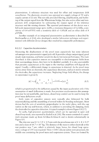
in capacitance is given by
1 1 x
2
2
x <<
∆C =ε A − → ε2 A (8.5)
d 0
d − x d + d 2 0
x
0
0
which is proportional to the deflection caused by the input acceleration only if the
assumption of small deflections is made. For precision accelerometers this assump-
tion may be not justifiable, and hence, closed loop control can be used to keep the
proof mass deflections small.
Early types of capacitive sensors were typically also fabricated by bulk
micromachining and the assembling of several wafers by bonding techniques. Most
devices had the axis of sensitivity perpendicular to the wafer plane, with the cap
wafers on the top and bottom, which, in addition to providing the damping, form
the electrodes for capacitive detection. A typical example is shown Figure 8.8 [17].
An early, high-precision accelerometer, which can be operated in open and
closed loop mode, was reported by Rudolf et al. [18]. The sensor consisted of a sand-
wich structure made up from Si-Glass-Si-Glass-Si and is shown schematically in
Figure 8.9.
The chip size was 8.3 × 5.9 × 1.9 mm with the proof mass size of 4 × 4 × 0.37
–6
mm and a mass of 14.7 × 10 kg. The distance of the mass to either electrode at the
rest position was 7 µm, which is relatively large; hence, for closed loop opera-
tion a voltage of 15V was required. Three <100> silicon wafers were processed, the
middle one containing the proof mass and suspension system. These are formed by

