
Page 118 - MEMS and Microstructures in Aerospace Applications
P. 118
Osiander / MEMS and microstructures in Aerospace applications DK3181_c005 Final Proof page 106 25.8.2005 3:39pm
106 MEMS and Microstructures in Aerospace Applications
Surface
Anchor SiO 2 Bottom electrode
membrane membrane spacer 2.5 µm
(polysilicon)
5 µm
Substrate
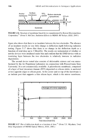
FIGURE 5.16 Structure of membrane-based device manufactured by Boston Micromachines
Corporation. 17 (From S. McClure, Radiation Effects in MEMS: RF Relays, IEEE, 2003.)
figure also shows that there is no insulator between the two electrodes. The absence
of an insulator results in very little change in deflection depth following radiation
testing. Figure 5.17 shows that there is no change in the deflection depth as a
function of total dose up to 3 Mrad(Si). The results are independent of whether or
not the devices were irradiated under bias and confirm that the DMD device with no
insulating layer between the two electrodes is relatively immune to radiation
degradation.
The second device tested also consists of deformable mirrors and was manu-
factured by the Jet Propulsion Laboratory in conjunction with Pennsylvania State
University. It is not commercially available. A piezoelectric membrane, comprised
of a layer of lead zirconium titanate (PZT) deposited on silicon nitrite, is anchored
at two opposite edges to silicon posts. At the center and on top of the membrane is
an indium post that supports a thin silicon layer, which is the mirror membrane.
2.0
Average of 5 mirror segments
Deflection depth at 140 V (µm) 1.6
1.8
1.4
1.2
1.0
0 500 1000 1500 2000 2500 3000
Total dose [krad/(Si)]
FIGURE 5.17 Plot of deflection depth as a function of dose. 17 (From T.F. Miyahara, Total
Dose Degradation of MEMS Optical Mirrors, IEEE, 2003.)
© 2006 by Taylor & Francis Group, LLC