
Page 116 - MEMS and Microstructures in Aerospace Applications
P. 116
Osiander / MEMS and microstructures in Aerospace applications DK3181_c005 Final Proof page 104 25.8.2005 3:39pm
104 MEMS and Microstructures in Aerospace Applications
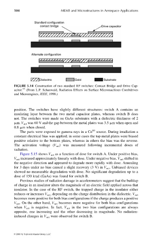
Standard configuration
contact bridge Drive capacitor
Alternate configuration
Dielectric Gold Substrate
FIGURE 5.14 Construction of two standard RF switches: Contact Bridge and Drive Cap-
acitor. 16 (From L.P. Schanwald, Radiation Effects on Surface Micromachines Combdrives
and Microengines, IEEE, 1998.)
position. The switches have slightly different structures: switch A contains an
insulating layer between the two metal capacitor plates, whereas switch B does
not. The switches were made on GaAs substrates with a dielectric thickness of 2
mm. V act was 60 V and the gap between the metal plates was 3.5 mm when open and
0.8 mm when closed.
60
The parts were exposed to gamma rays in a Co source. During irradiation a
constant electrical bias was applied; in some cases the top metal plates were biased
positive relative to the bottom plates, whereas in others the bias was the reverse.
The activation voltage (V act ) was measured following incremental doses of
radiation.
Figure 5.15 shows V act as a function of dose for switch A. Under positive bias,
V act increased approximately linearly with dose. Under negative bias, V act shifted in
the negative direction and appeared to degrade more rapidly with dose. Annealing
for 3 days under no bias caused a slight recovery (3 V) in V act . Unbiased devices
showed no measurable degradation with dose. No significant degradation up to a
dose of 150 krad (GaAs) was found for switch B.
Previous studies of radiation damage in accelerometers suggest that the buildup
of charge in an insulator alters the magnitude of an electric field applied across that
insulator. In the case of the RF switch, the trapped charge in the insulator either
reduces or increases V act , depending on the charge distribution in the dielectric. V act
becomes more positive for both bias configurations if the charge produces a positive
V act . On the other hand, V act becomes more negative for both bias configurations
when V act is negative. In fact, V act in the two bias configurations are always
opposite, one increasing and the other decreasing in magnitude. No radiation-
induced changes in V act were observed for switch B.
© 2006 by Taylor & Francis Group, LLC