
Page 112 - MEMS and Microstructures in Aerospace Applications
P. 112
Osiander / MEMS and microstructures in Aerospace applications DK3181_c005 Final Proof page 100 25.8.2005 3:39pm
100 MEMS and Microstructures in Aerospace Applications
beam X moves relative to beams Y and Z so that C 1 6¼ C 2 . The result is an AC
voltage on X, which is demodulated and compared with a reference voltage in the
buffer amplifier. The difference between the two voltages is a measure of
the acceleration and appears at the device’s output. Beam X is electrically tied
to the substrate to prevent the arms from bending down towards the substrate in the
presence of a voltage difference between the beam X and the substrate. This effect
would lead to an erroneous voltage reading on the output.
The first experiment involved irradiating the entire device with 65 MeV protons
and monitoring the outputs of the preamplifier (V pr ) and of the buffer amplifier
(V out ). Proton irradiation caused both V pr and V out to change, but in opposite
directions. Furthermore, the dose rate had a significant effect on both the magnitude
and direction of change. These results were not too surprising given that the
ADXL50 contained CMOS control circuits that are known to be radiation-sensitive.
With an aperture placed over the accelerometer to cover the electronic circuit
and expose only the mechanical part to ion beam irradiation, it was possible to
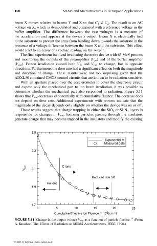
determine whether the mechanical part also responded to radiation. Figure 5.11
shows that V out decreases exponentially with cumulative fluence. The decrease does
not depend on dose rate. Additional experiments with protons indicate that the
magnitude of the decay depends only slightly on whether the device was on or off.
These results suggest that charge trapping in either the SiO 2 or Si 3 N 4 layers is
responsible for changes in V out . Ionizing particles passing through the insulators
generate charge that may become trapped in the insulators and modify the existing
2.5
Exponential fit
Measured data
2.3
V out 2.1 C ions
Reduced rate 5X
He ions
1.9
1.7
0 5 10 15 20 25
9
−2
Cumulative Effective lon Fluence 10 (cm )
FIGURE 5.11 Change in the output voltage V out as a function of particle fluence. 13 (From
A. Knudson, The Effects of Radiation on MEMS Accelerometers, IEEE, 1996.)
© 2006 by Taylor & Francis Group, LLC