
Page 111 - MEMS and Microstructures in Aerospace Applications
P. 111
Osiander / MEMS and microstructures in Aerospace applications DK3181_c005 Final Proof page 99 25.8.2005 3:39pm
Space Radiation Effects and Microelectromechanical Systems 99
C 1 C 2
Y X Z
d
d 1 2
0.2 V 1.8 V 3.4 V 2 µm
1.6 µm
600 Å Si N
3 4
1.8 V 1200 Å Sio 2
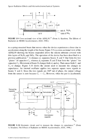
FIGURE 5.9 Cross-sectional view of the ADXL50. 13 (From A. Knudson, The Effects of
Radiation on MEMS Accelerometers, IEEE, 1996.)
to a spring-mounted beam that moves when the device experiences a force due to
acceleration along the length of the beam. Figure 5.9 is a cross-sectional view of the
ADXL50 showing the beams suspended above the silicon substrate covered with
thin layers of Si 3 N 4 and SiO 2 . The operation of the device has been described in a
previous publication. 13 A distance d 1 separates beams X and Y that form the two
‘‘plates’’ of capacitor C 1 , whereas d 2 separates X and Z that form the ‘‘plates’’ for
capacitor C 2 . Movement of beam X changes both d 1 and d 2 . That causes both C 1 and
C 2 to change. Figure 5.10 shows the circuit used to measure the changes in
capacitance. An internal oscillator applies two separate square wave signals to
beams Y and Z. Since the two signals are 1808 out of phase, the output voltage
from the sensor is zero because C 1 ¼ C 2 . However, when the part is accelerated,
3.4 V 3.4 V
Reference 6 V
ref
Feedback
1.8 V
Decoupling
capacitor
4 Oscillator Sensor Demodulator
Preamp Buffer
amp
ST 7
5 1 2 3 8 10 9
V
pr
5 V Demodulator
capacitor
V
out
FIGURE 5.10 Electronic circuit used to measure the changes in capacitance. 13 (From
A. Knudson, The Effects of Radiation on MEMS Accelerometers, IEEE, 1996.)
© 2006 by Taylor & Francis Group, LLC