
Page 117 - MEMS and Microstructures in Aerospace Applications
P. 117
Osiander / MEMS and microstructures in Aerospace applications DK3181_c005 Final Proof page 105 25.8.2005 3:39pm
Space Radiation Effects and Microelectromechanical Systems 105
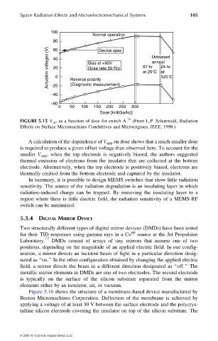
100
Normal operation
80 Device spec
Actuation voltages (V) 40 0 Reverse polarity 67 hr Unbiased
60
anneal
Bias at +90V
24 hr
20
Dose rate 50 R/s
at 25 C at
125 C
−20
−40 (Diagnostic measurement)
−60
0 50 100 150 200 250 300
Dose [krd(GaAs)]
FIGURE 5.15 V act as a function of dose for switch A. 16 (From L.P. Schanwald, Radiation
Effects on Surface Micromachines Combdrives and Microengines, IEEE, 1998.)
A calculation of the dependence of V app on dose shows that a much smaller dose
is required to produce a given offset voltage than observed here. To account for the
smaller V app , when the top electrode is negatively biased, the authors suggested
thermal emission of electrons from the insulator that are collected at the bottom
electrode. Alternatively, when the top electrode is positively biased, electrons are
thermally emitted from the bottom electrode and captured by the insulator.
In summary, it is possible to design MEMS switches that show little radiation
sensitivity. The source of the radiation degradation is an insulating layer in which
radiation-induced charge can be trapped. By removing the insulating layer to a
region where there is little electric field, the radiation sensitivity of a MEMS RF
switch can be minimized.
5.3.4 DIGITAL MIRROR DEVICE
Two structurally different types of digital mirror devices (DMDs) have been tested
for their TID responses using gamma rays in a Co 60 source at the Jet Propulsion
Laboratory. 17 DMDs consist of arrays of tiny mirrors that assume one of two
positions, depending on the magnitude of an applied electric field. In one config-
uration, a mirror directs an incident beam of light in a particular direction desig-
nated as ‘‘on.’’ In the other configuration obtained by changing the applied electric
field, a mirror directs the beam in a different direction designated as ‘‘off.’’ The
metallic mirror elements in DMDs are one of two electrodes. The second electrode
is typically on the surface of the silicon substrate separated from the mirror
elements either by an insulator, air, or vacuum.
Figure 5.16 shows the structure of a membrane-based device manufactured by
Boston Micromachines Corporation. Deflection of the membrane is achieved by
applying a voltage of at least 30 V between the surface electrode and the polycrys-
talline silicon electrode covering the insulator on top of the silicon substrate. The
© 2006 by Taylor & Francis Group, LLC