
Page 425 -
P. 425
7-14 MEMS: Design and Fabrication
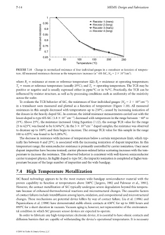
1
Resistor 1 (trans)
0.95 Resistor 2 (long)
Normalized resistance 0.85 Resistor 4 (long)
Resistor 3 (trans)
0.9
0.8
0.75
0.7
0.65
0 50 100 150 200 250
Temperature (°C)
FIGURE 7.10 Change in normalized resistance of four individual gauges in a transducer as function of tempera-
19
3
ture. All measured resistances decrease as the temperature increases (n 6H-SiC, N 2 10 /cm ).
d
where R resistance at room or reference temperature (Ω); R resistance at operating temperature;
o f
T room or reference temperature (usually 25°C); and T operating temperature. The TCR may be
o f
positive or negative and is usually expressed either in ppm/°C or in %/°C. Practically, the TCR can be
influenced by resistor structure, as well as by processing conditions such as uniformity of the resistivity
across the wafer.
3
19
To evaluate the TCR behavior of SiC, the resistances of four individual gauges (N 2 10 cm )
d
in a transducer were measured and plotted as a function of temperature (Figure 7.10). All measured
resistances in this sample decreased with temperatures up to 250°C, caused by increasing ionization of
the donors in the heavily doped SiC. In contrast, the initial resistance measurements carried out with the
17
3
lower-doped n-type 6H-SiC (1.8 10 cm ) decreased with temperature in the range between 60° to
25°C. Above 25°C, the resistance increased. Using Equation (7.12), the average TCR value for the range
18
25 to 625°C was found to be 0.56%/°C. In the 3 10 cm 3 doped samples, the resistance was observed
to decrease up to 100°C and then begin to increase. The average TCR value for this sample in the range
100 to 625°C was found to be 0.28%/°C.
The decrease in resistance with increase of temperature below a certain temperature limit, which typ-
ically lies between 0 and 25°C, is associated with the increasing ionization of dopant impurities. In this
temperature range, the semiconductor resistance is primarily controlled by carrier ionization. Once most
dopant impurities have become ionized, carrier phonon-related lattice scattering increases with the tem-
perature to increase the resistance. This observed behavior is consistent with well-known semiconductor
carrier transport physics. In highly doped n-type SiC, the impurity ionization is completed at higher tem-
perature because of the large number of impurities and the wide bandgap.
7.4 High Temperature Metallization
SiC-based technology appears to be the most mature wide-bandgap semiconductor material with the
proven capability to function at temperatures above 500°C [Jurgens, 1982 and Palmour et al., 1991].
However, the contact metallization of SiC typically undergoes severe degradation beyond this tempera-
ture because of enhanced thermochemical reactions and microstructural changes. The causative factors
of contact failures include interdiffusion among layers, oxidation, and compositional and microstructural
changes. These mechanisms are potential device killers by way of contact failure. Liu et al. (1996) and
Papanicolaou et al. (1998) have demonstrated stable ohmic contacts at 650°C for up to 3000 hours and
850°C for a short duration in vacuum. Vacuum aging is, however, not representative of the environmen-
tal condition in which SiC pressure sensor devices are expected to operate.
In order to fabricate any high-temperature electronic device, it is essential to have ohmic contacts and
diffusion barriers that are capable of withstanding the device’s operational temperatures. It is necessary
© 2006 by Taylor & Francis Group, LLC