
Page 426 -
P. 426
Single-Crystal Silicon Carbide MEMS: Fabrication, Characterization, and Reliability 7-15
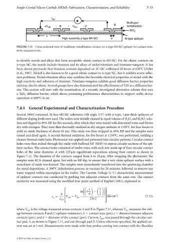
I AD
Multilayer
D
+V − B + V − C metallization
AB BC
SiO 2
s
High resistivity p-type 6H-SiC d N-type epilayer
FIGURE 7.11 Cross-sectional view of multilayer metallization contact on n-type 6H-SiC epilayer for contact resis-
tivity measurements.
to identify metals and alloys that form acceptable ohmic contact to 6H-SiC. For the ohmic contacts on
n-type SiC, the metals include titanium and its alloys of nickel–titanium and titanium–tungsten. It has
been shown previously that titanium contacts deposited on 3C-SiC withstand 20 hours at 650°C [Zeller
et al., 1987]. Nickel is also known to be a good ohmic contact to n-type SiC, but it exhibits severe adhe-
sion problems. Nickel–titanium alloys may combine the favorable electrical properties of nickel with the
high reactivity and adhesion of titanium. Titanium–tungsten exhibits good diffusion barrier properties
and may also be ohmic. Several groups have also demonstrated the effectiveness of TiN as a diffusion bar-
rier. This section will start with the examination of a recently investigated alternative scheme that uses
a TaSi diffusion barrier, which shows promising performance characteristics to support stable device
2
operation at 600°C in air.
7.4.1 General Experimental and Characterization Procedure
Several (0001)-oriented, Si-face 6H-SiC substrates (tilt angle 3.5°) with n-type, 1µm-thick epilayers of
different doping levels were used. The wafers were initially cleaned in equal volume of H O and H SO solu-
2 2 2 4
tion and dipped in 49% HF for five seconds, after which they were rinsed with deionized water and blown
dry with nitrogen. They were then thermally oxidized in dry oxygen ambient at 1150°C for four hours to
yield an oxide thickness of about 60 nm. This oxide was then stripped in 49% HF and the samples were
rinsed and dried again. A second thermal oxidation, for five hours at 1150°C, was performed, yielding a
cleaner thermal oxide layer. Photoresist was applied and patterned into circular patterns. Circular contact
holes were then etched through the oxide with buffered HF (BHF) to expose circular sections of the epi-
layer surface. The contact holes consisted of twelve rows, with each row made up of four circular contact
holes of the same diameter, d, with 225µm equidistant separations among their centers as shown in
Figure 7.11. The diameter of the contacts ranged from 6 to 28 µm. After stripping the photoresist, the
samples were RCA-cleaned again, but with no HF dip, to ensure that a very clean epilayer surface with a
monolayer of oxide was formed. The samples were immediately transferred into the sputtering chamber
for metal depositions. A 300°C dehydration process, in vacuum for 20 minutes, followed, to remove any
water trapped within micropipes in the wafers. The Current–Voltage (I–V) characteristic measurement
of epilayer contacts was conducted by probing two adjacent contacts from the same row. The contact
resistivity was measured using the modified four-point method of Kuphal (1981), expressed as
cs ln 3
s
1
2
d
A
2
r V AB V BC 2ln2 [Ω-cm ] (7.13)
I
AD
where V is the voltage measured across contacts A and B in Figure 7.11, whereas V measures the volt-
AB BC
age between contacts B and C (epilayer resistance); A contact area (µm); s distance between adjacent
contacts (µm); and d diameter of the contact (µm). Current, I , was passed through the circular con-
AD
tact pad, A, as shown in Figure 7.11, and out through pad D. Unless otherwise specified, the applied cur-
rent was set at 1 mA. Measurements were made with four probes coming into contact with the Shockley
© 2006 by Taylor & Francis Group, LLC