
Page 429 -
P. 429
7-18 MEMS: Design and Fabrication
direct contact with the epilayer. The synchronous tracking of Ti and C atoms at a constant ratio of almost
1:2 (discounting the primary Ti–N signal that was difficult to distinguish) strongly suggested the forma-
tion of aTiC species. Several groups had previously confirmed the formation of TiC and Ti Si species
1-x 5 3
for wafers annealed in the range of 500 to 1200°C. The decrease in the SBH could be associated with the
low work function of TiC (3.35eV) compared to that of titanium (4.1eV) (1976).
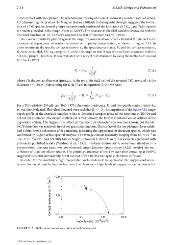
The contact resistivity plotted against the impurity concentration, which exhibited the characteristic
exponential dependence of contact resistivity on impurity concentration, is shown in Figure 7.13. In
order to estimate the specific contact resistivity, r , the spreading resistance, R , and the contact resistance,
cs
s
R ,were decoupled. TiC was assigned R on the assumption that it was the new layer in contact with the
c s
6H-SiC epilayer. Therefore, R was evaluated with respect to its thickness by using the method of Cox and
s
H. Strack (1967):
t
R ρ (7.16)
s TiC d 2
π( )
2
where d is the contact diameter (µm), ρ is the resistivity (µΩ-cm) of the assumed TiC layer, and t is the
TiC
thickness ( 100nm). Substituting for R in (7.16) in Equation (7.14), we have:
s
t 1
ρ TiC R [V AB V ] (7.17)
c
BC
π( ) I AD
d 2
2
For a TiC resistivity 200µΩ-cm [Toth, 1971], the contact resistance, R , and the specific contact resistivity,
c
ρ , was then evaluated. The values obtained were such that R R .A comparison of the Figure 7.12 Auger
c s c
depth profile of the annealed samples to the as-deposited samples revealed the reactions at TiN/Pt and
6H-SiC/Ti interfaces. The oxygen content (at. 17%) between the former interfaces was an artifact of the
deposition system. The degree of its effect on the electrical characteristics was not known, but the 6H-
SiC/Ti interface was relatively free of oxygen contamination. The surface of the top platinum layer exhib-
ited a faint brown coloration after annealing, indicating the appearance of titanium species, which was
confirmed by Auger surface spectral analysis. The average contact resistivity, ranging from 1.5 10 5 to
2
3.42 10 4 Ω-cm , and Schottky barrier height, between 0.8–0.84 eV, were in reasonable agreement with
previously published results [Waldrop et al., 1993]. Interlayer delamination, sometimes attendant in a
pre-processed titanium layer, was not observed. Auger Electron Spectroscopy (AES) revealed the out-
diffusion of titanium-silicon species. The continued presence of the TiN layer after annealing at 1000°C
suggested its partial survivability, but it did not offer a full barrier against platinum diffusion.
In order for this multilayer, high-temperature metallization to be applicable, the oxygen contamina-
tion in the metal must be kept to less than 3 at. % oxygen. High levels of oxygen contamination at the
10.0
Contact resistance (Ω10 −4 cm 2 ) 1.0
0.1
0.0 0.1 1.0 10.0
19 −3
Impurity conc. (10 cm )
FIGURE 7.13 Bulk contact resistance as function of doping level.
© 2006 by Taylor & Francis Group, LLC