
Page 430 -
P. 430
Single-Crystal Silicon Carbide MEMS: Fabrication, Characterization, and Reliability 7-19
interfaces of Pt/TiN or TiN/Ti could be the result of full or partial decomposition of the titanium nitride
layer at high temperature and replacement by a layer of titanium oxide, caused by the high affinity of tita-
nium toward oxygen.
Formation of titanium oxide results in two deleterious effects: (a) it greatly reduces the effectiveness of
the diffusion barrier, and (b) it forms a dielectric layer, which leads to rectification and failure of the ohmic
contact. Another destructive effect is penetration of oxygen through the outer platinum layer. Inspection
with scanning electron microscope (SEM) indicated that the deposited platinum layer contained a high
density of pinholes. At high temperature, oxygen would diffuse through the pinholes, thereby degrading
the titanium nitride diffusion barrier. Oxygen also reacts with the titanium beneath the barrier, forming
a solid titanium oxide layer with undesirable rectifying properties that extends to the 6H-SiC surface. For
the metallization scheme to work effectively in air, the issue of oxygen contamination must be resolved.
7.4.3 Ti/TaSi /Pt Scheme
2
Oxygen contamination generally posed a big problem for the Ti/TiN/Pt scheme, but the problem is min-
imized if the device with such metallization is hermetically sealed. However, the diffusion barrier integrity
of the TiN layer against platinum diffusion to the semiconductor interface is also undesirable. A robust,
high-temperature metallization scheme must have, at a minimum, the following attributes: (a) ohmic
contact with reasonably low contact resistance relative to the bulk epilayer; (b) long-term contact stability
in the harsh environment; (c) compatibility with SiC large-scale integrated electronics fabrication tech-
nology; (d) good wire-bond strength; and (e) compatibility with high-temperature interconnect and
packaging technology.
In order to meet these criteria, it was necessary to identify metallization schemes that will both form
an ohmic contact on n-type SiC and offer an excellent diffusion barrier against both oxygen penetration
and migration of any top layer metallization, such as platinum, toward the contact SiC interface. In addi-
tion, such a scheme should have a top surface that is essentially wire-bondable. In developing this new
scheme, thermodynamic and thermochemical issues were taken into consideration with the recognition
that at 600°C, the activation energies of several metals are enough to promote reactions or intermixing
among metals. Metal layers with low mutual diffusivities were identified in order to keep intermixing
at a minimum. In the case where they mix, however, the alloys formed must be thermodynamically,
mechanically, and electrically stable. They must maintain excellent diffusion barrier characteristics. By
combining the ability of titanium to form ohmic contact on n-type SiC, the diffusion barrier character-
istics of TaSi , and the relative stability of the interface of the two layers, a new scheme was developed with
2
a result that proved far superior to the Ti/TiN scheme.
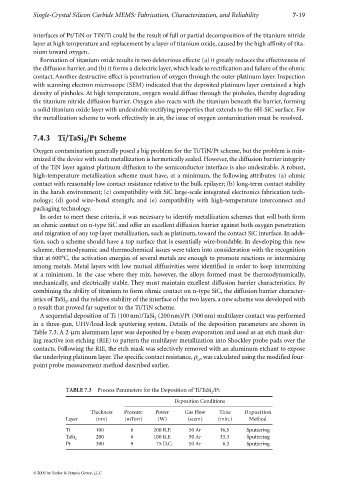
A sequential deposition of Ti (100 nm)/TaSi (200nm)/Pt (300 nm) multilayer contact was performed
2
in a three-gun, UHV/load-lock sputtering system. Details of the deposition parameters are shown in
Table 7.3. A 2-µm aluminum layer was deposited by e-beam evaporation and used as an etch mask dur-
ing reactive ion etching (RIE) to pattern the multilayer metallization into Shockley probe pads over the
contacts. Following the RIE, the etch mask was selectively removed with an aluminum etchant to expose
the underlying platinum layer. The specific contact resistance, ρ , was calculated using the modified four-
cs
point probe measurement method described earlier.
TABLE 7.3 Process Parameters for the Deposition of Ti/TaSi /Pt
2
Deposition Conditions
Thickness Pressure Power Gas Flow Time Deposition
Layer (nm) (mTorr) (W) (sccm) (min.) Method
Ti 100 6 200 R.F. 50 Ar 16.5 Sputtering
TaSi 2 200 6 100 R.F. 50 Ar 33.3 Sputtering
Pt 300 9 75 D.C. 50 Ar 6.3 Sputtering
© 2006 by Taylor & Francis Group, LLC