
Page 427 -
P. 427
7-16 MEMS: Design and Fabrication
pads that extend over the oxide. Therefore, the spreading and contact resistance, R and R , respectively,
s c
can be calculated by
V V
BC
AB
R R (7.14)
c
s
I
AD
The resistance of the probes in these measurements was negligible. Since the main parameter of interest in
these measurements was the overall change in resistance under the contact, R and R were lumped together
c s
in determining the contact resistivity.As a result of the lumping together of the spreading and contact resist-
ances, the result was considered to be on the high end of the average specific contact resistivity.
7.4.2 Characterization of Ti/TiN/Pt Metallization
Several (0001)-oriented, highly resistive, Si-face, p-type 6H-SiC substrates, each with n-type epilayers
19
17
3
(1µm thick) of different doping levels ranging between 3.3 10 cm 3 and 1.9 10 m , were pur-
chased from Cree Research, Inc. The wafers were initially cleaned by modified RCA method and dipped
in 49% HF for five seconds, followed by rinsing and blow-drying.An ex situ dehydration process, at 200°C
in nitrogen ambient for 20 minutes to desorb water trapped within the micropipes, followed this cleaning
process. Depositions of Ti (50nm)/TiN (50nm)/Pt (100nm) were made on the samples by sputtering
without breaking vacuum.Titanium nitride was obtained by reactive sputtering of titanium in 20% nitrogen/
argon ambient. The top platinum layer was etched in light aqua regia to form rectangular and circular
probe pads that overlapped the field oxide. The exposed TiN/Ti on the field oxide was selectively etched
in 1:1 EDTA:H O to electrically isolate. The pads offered total coverage of the contact regions and facil-
2
2
itated broad area probe contact during testing. In the as-deposited state, the titanium contact on the n-
3
19
type epilayer was ohmic for the sample with the highest doping level (1.9 10 cm ). The contact
5
resistance using Equation (7.13) was found to be approximately 1 10 cm . In order to obtain ohmic
18
17
3
contact to n-type 6H-SiC with lower doping levels (3.3 10 –10 cm ), high-temperature annealing
was required.
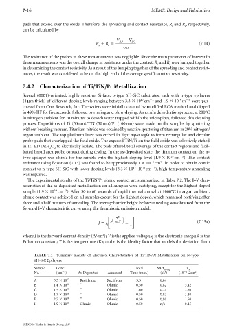
The experimental results of the Ti/TiN/Pt ohmic contact are summarized in Table 7.2. The I–V char-
acteristics of the as-deposited metallization on all samples were rectifying, except for the highest doped
19
3
sample (1.9 10 cm ). After 30 to 60 seconds of rapid thermal anneal at 1000°C in argon ambient,
ohmic contact was achieved on all samples except for the lightest doped, which remained rectifying after
three and a half minutes of annealing. The average barrier height before annealing was obtained from the
forward I–V characteristic curve using the thermionic emission model:
qV
s 1
J J e nkT (7.15a)
2
where J is the forward current density (A/cm ); V is the applied voltage; q is the electronic charge; k is the
Boltzman constant; T is the temperature (K); and n is the ideality factor that models the deviation from
TABLE 7.2 Summary Results of Electrical Characteristics of Ti/TiN/Pt Metallization on N-type
6H-SiC Epilayers
Sample Conc. Total SBH as-dep r cs
3
2
4
No. (cm ) As-Deposited Annealed Time (min.) (eV) (10 Ωcm )
A 3.3 10 17 Rectifying Rectifying 3.5 0.84
B 1.4 10 18 ” Ohmic 0.50 0.82 3.42
C 1.5 10 18 ” Ohmic 1.00 0.74 2.50
D 1.7 10 18 ” Ohmic 0.50 0.82 2.10
E 2.7 10 18 ” Ohmic 0.50 0.80 1.50
F 1.9 10 19 Ohmic Ohmic 0.50 n/a 0.15
© 2006 by Taylor & Francis Group, LLC