
Page 140 - Make Your Own PCBs with EAGLE from Schematic Designs to Finished Boards
P. 140
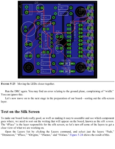
FIGURE 5-23   Moving the LEDs closer together.


      Run the DRC again. You may find an error relating to the ground plane, complaining of “width.”
  You can ignore this.

      Let’s now move on to the next stage in the preparation of our board—sorting out the silk-screen
  layer.


  Text on the Silk Screen


  To make our board look really good, as well as making it easy to assemble and see which component
  goes where, we need to sort out the writing that will appear on the board, known as the silk screen.
  The “tPlace” is the layer responsible for the silk screen, so let’s turn off some of the layers to get a
  clear view of what we are working on.

      Open  the  Layers  list  by  clicking  the  Layers  command,  and  select  just  the  layers  “Pads,”
  “Dimension,” “tPlace,” “tOrigins,” “tNames,” and “tValues.” Figure 5-24 shows the result of this.