
Page 142 - Make Your Own PCBs with EAGLE from Schematic Designs to Finished Boards
P. 142
• Delete the 1N4148 value on D1.
The fonts are all different, so we will use the Change tool to change all the labels to be of size
0.05 and font type Vector. Generally, it is better to use the Vector font everywhere on the board. This
will guarantee that the text on the actual board will look like the text in the Board Editor.
Click on the Change command (the icon looks like a wrench). Change only changes the last setting
that you make in the Change menu. On the menu, you will see “Size.” Change this to be 0.05. Select
the Group tool, select the whole board, and then right-click and do “Group: Change.”
Repeat the process but setting each label to be the Vector font by selecting “Font” and then
“Vector” from the Change menu. Then again, set the “Ratio” to be 12.
Finally, repeat the process one last time using the Change tool to set the “Layer” of all the labels
and component outlines to be “tPlace” because this is the layer that we will use for the silk screen.
Note that this is probably best not done as a Group selection unless you are very careful not to select
the board outline, which is in the “Dimension” layer and needs to remain on this layer.
Drag the labels about so that they don’t overlap. Note that to move, you must have the Origins
layer selected.
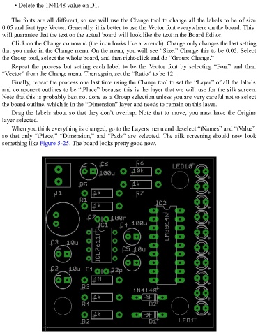
When you think everything is changed, go to the Layers menu and deselect “tNames” and “tValue”
so that only “tPlace,” “Dimension,” and “Pads” are selected. The silk screening should now look
something like Figure 5-25. The board looks pretty good now.