
Page 154 - Make Your Own PCBs with EAGLE from Schematic Designs to Finished Boards
P. 154
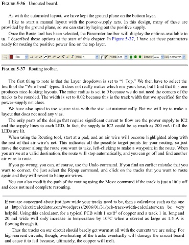
FIGURE 5-36   Unrouted board.


      As with the automated layout, we have kept the ground plane on the bottom layer.
      I  like  to  start  a  manual  layout  with  the  power-supply  nets.  In  this  design,  many  of  these  are
  provided by the ground plane, so we can start by laying out the positive supply.

      Once the Route tool has been selected, the Parameter toolbar will display the options available to
  us. I described these options at the start of this chapter. In Figure 5-37, I have set these parameters
  ready for routing the positive power line on the top layer.


  FIGURE 5-37   Routing toolbar.


      The first thing to note is that the Layer dropdown is set to “1 Top.” We then have to select the
  fourth of the “Wire bend” types. It does not really matter which one you chose, but I find that this one
  produces nice-looking layouts. The miter radius is set to 0 because we do not need the corners of the
  tracks to be rounded. The width is set to 0.02 because this is the track width that we specified for the

  power-supply net class.
      We have also opted to use square vias with the size set automatically. But we will try to make a
  layout that does not need any vias.

      The only parts of the design that require significant current to flow are the power supply to IC2
  and the supply lines to each LED. In fact, the supply to IC2 could be as much as 200 mA if all the
  LEDs are lit.

      When using the Routing tool, start at a pad, and an air wire will become highlighted along with
  the rest of that air wire’s net. This indicates all the possible target points for your routing, so just
  move the cursor along the route you want to take, left-clicking to make a waypoint in the route. When
  you arrive at a valid destination, the route will stop automatically, and you can go off and find another
  air wire to route.

      If you go wrong, you can, of course, use the Undo command. If you find an earlier mistake that you
  want to correct, the just select the Ripup command, and click on the tracks that you want to route
  again and they will revert to being air wires.

      You can also modify the path of the routing using the Move command if the track is just a little off
  and does not need complete rerouting.


    If you are concerned about just how wide your tracks need to be, then a calculator such as the one
    at  http://circuitcalculator.com/wordpress/2006/01/31/pcb-trace-width-calculator/can  be  very
                                                                            2
    helpful. Using this calculator, for a typical PCB with 1 oz/ft  of copper and a track 1 in. long and
    20  mil  wide  will  only  increase  in  temperature  by  10°C  when  a  current  as  large  as  1.5 A  is
    flowing through it.
         Thus the tracks on our circuit should barely get warm at all with the currents we are using. For
    high-current circuits, though, overheating of the tracks eventually will damage the circuit board

    and cause it to fail because, ultimately, the copper will melt.