
Page 152 - Make Your Own PCBs with EAGLE from Schematic Designs to Finished Boards
P. 152
Now that we have all the components swapped over to SMD equivalents, we need to do a bit of
tidying up and reroute the board.
Resize and Tidy the Board
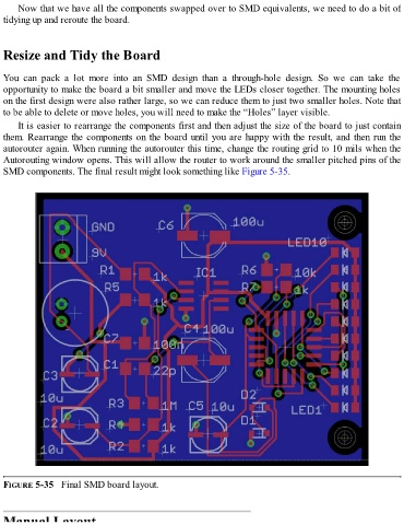
You can pack a lot more into an SMD design than a through-hole design. So we can take the
opportunity to make the board a bit smaller and move the LEDs closer together. The mounting holes
on the first design were also rather large, so we can reduce them to just two smaller holes. Note that
to be able to delete or move holes, you will need to make the “Holes” layer visible.
It is easier to rearrange the components first and then adjust the size of the board to just contain
them. Rearrange the components on the board until you are happy with the result, and then run the
autorouter again. When running the autorouter this time, change the routing grid to 10 mils when the
Autorouting window opens. This will allow the router to work around the smaller pitched pins of the
SMD components. The final result might look something like Figure 5-35.
FIGURE 5-35 Final SMD board layout.
Manual Layout