
Page 148 - Make Your Own PCBs with EAGLE from Schematic Designs to Finished Boards
P. 148
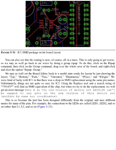
FIGURE 5-31   IC1 SMD package on the board layout.


      You can also see that the routing is now, of course, all in a mess. This is only going to get worse,
  so  we  may  as  well  go  back  to  air  wires  by  doing  a  group  ripup.  To  do  this,  click  on  the  Ripup
  command, then click on the Group command, drag over the whole area of the board, and right-click
  and slect the option “Ripup: Group.”

      We may as well set the Board Editor back to a useful state ready for layout by just showing the
  layers  “Top,”  “Bottom,”  “Pads,”  “Vias,”  “Unrouted,”  “Dimension,”  “tPlace,”  and  “tOrigin.”  We
  were kind of lucky with IC1 in that there was a drop-in SMD replacement using the same pin names.
  Unfortunately, things are not quite so easy for IC2. Using the Replace tool and a search string of
  “*3914V*” will find an SMD equivalent of the chip, but when we try to do the replacement, we will

  get an error message Date A in the old version of device set LM3914N can’t
  be  mapped  to  any  gate  in  the  new  version  of  this  device  set
  (neither by name nor coordinates).
      This  is  so  because  the  part  has  been  designed  differently  from  the  original  and  uses  different

  names for many of the pins. For example, the connections to the LEDs are called LED1, LED2, and so
  on rather than L1, L2, and so on (Figure 5-32).