
Page 209 - Make Your Own PCBs with EAGLE from Schematic Designs to Finished Boards
P. 209
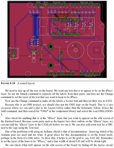
FIGURE 8-10   A routed layout.


      We need to tidy up all the text on the board. We want any text that is to appear to be on the tPlace
  layer. So use the Smash command to separate all the labels from their parts, and then use the Change
  command to set the layer of the text that you want to keep to be tPlace.

      Now use the Change command to make all the labels a Vector font and then set their size to 0.032.
      Because this is an OSH project, we should also put the OSH logo on the board. This is a rare

  occasion where we can add a part to the Layout Editor rather than the Schematic Editor. Select the
  Add command, and then search for *OSH* in the component library and select the icon OSH-LOGO-
  L.
      Also check for anything that is in the “tDocu” layer that you want to appear on the silk screen of
  the finished board. Because some parts such as the buzzer have their outline on the “tDocu” layer, we

  can just add the “tDocu” layer to the CAM job before we run it. We can also add some text for a URL
  next to the logo using the Text tool.
      One of the problems with using an Arduino shield is that of documentation—knowing which of the

  Arduino  pins  are  used  and  for  what. A  great  place  for  this  documentation  is  on  the  board  itself,
  perhaps in the form of a little table. To draw this, it helps to set the grid to, say, 0.01 mil. Remember
  to set the layer of the lines to be “tPlace,” and a line width of about 0.05 mil will be about right.
      We can check what will appear on the silk screen of the board by hiding all the layers except