
Page 55 - Make Your Own PCBs with EAGLE from Schematic Designs to Finished Boards
P. 55
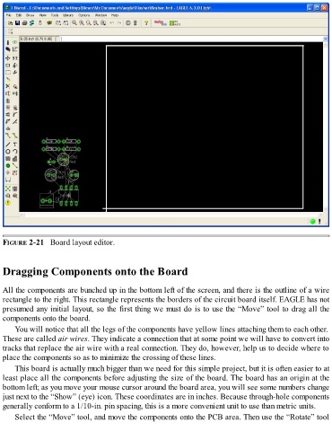
FIGURE 2-21   Board layout editor.


  Dragging Components onto the Board


  All the components are bunched up in the bottom left of the screen, and there is the outline of a wire
  rectangle to the right. This rectangle represents the borders of the circuit board itself. EAGLE has not
  presumed any initial layout, so the first thing we must do is to use the “Move” tool to drag all the
  components onto the board.

      You will notice that all the legs of the components have yellow lines attaching them to each other.
  These are called air wires. They indicate a connection that at some point we will have to convert into
  tracks that replace the air wire with a real connection. They do, however, help us to decide where to
  place the components so as to minimize the crossing of these lines.

      This board is actually much bigger than we need for this simple project, but it is often easier to at
  least place all the components before adjusting the size of the board. The board has an origin at the
  bottom left; as you move your mouse cursor around the board area, you will see some numbers change
  just next to the “Show” (eye) icon. These coordinates are in inches. Because through-hole components
  generally conform to a 1/10-in. pin spacing, this is a more convenient unit to use than metric units.

      Select the “Move” tool, and move the components onto the PCB area. Then use the “Rotate” tool