
Page 54 - Make Your Own PCBs with EAGLE from Schematic Designs to Finished Boards
P. 54
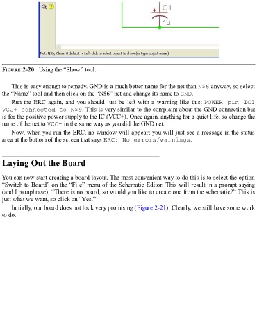
FIGURE 2-20   Using the “Show” tool.


      This is easy enough to remedy. GND is a much better name for the net than N$6 anyway, so select
  the “Name” tool and then click on the “N$6” net and change its name to GND.

      Run  the  ERC  again,  and  you  should  just  be  left  with  a  warning  like  this: POWER pin IC1
  VCC+ connected to N$9. This is very similar to the complaint about the GND connection but
  is for the positive power supply to the IC (VCC+). Once again, anything for a quiet life, so change the
  name of the net to VCC+ in the same way as you did the GND net.

      Now, when you run the ERC, no window will appear; you will just see a message in the status
  area at the bottom of the screen that says ERC: No errors/warnings.


  Laying Out the Board


  You can now start creating a board layout. The most convenient way to do this is to select the option
  “Switch to Board” on the “File” menu of the Schematic Editor. This will result in a prompt saying
  (and I paraphrase), “There is no board, so would you like to create one from the schematic?” This is
  just what we want, so click on “Yes.”

      Initially, our board does not look very promising (Figure 2-21). Clearly, we still have some work
  to do.