
Page 102 - Mechanical Engineers Reference Book
P. 102
Analogue and digital electronics theory 2/43
2.3.19 Boolean algebra A
The basiic rules of Boolean algebra are conveniently described
with reference to simple manually switched circuits. In the
binary notation a ‘0’ denotes that the switch is off and a ‘1’ that
the switch is on. The ‘0’ and ‘1‘ can also be taken to represent T B T
the absence or presence, respectively, of a voltage or a
current.
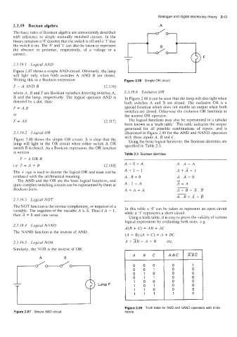
2.3.1 9.1 Logical AND
Figure 2.87 shows a simple AND circuit. Obviously. the lamp
will light only when both switches A AND B are closed.
Writing this as a Boolean expression Figure 2.88 Simple OR circuit
F=AANDB (2.116)
where A,, B and Fare Boolean variables denoting switches A, 2.3.19.6 Exclusive OR
B and the lamp, respectively. The logical operator AND is In Figure 2.88 it can be seen that the lamp will also light when
denoted by a dot, thus: both switches A and B are closed. The exclusive OR is a
F = A.B special function which does not enable an output when both
switches are closed. Otherwise the exclusive OR functions as
or the normal OR operator.
F= AB’ (2.117) The logical functions may also be represented in a tabular
form known as a ‘truth table’. This table indicates the output
generated for all possible combinations of inputs, and is
2.3.19.2 Logical OR illustrated in Figure 2.89 for the AND and NAND operators
with three inputs A, B and C.
Figure 2.88 shows the simple OR circuit. It is clear that the Using the basic logical functions, the Boolean identities are
lamp will light in the OR circuit when either switch A OR specified in Table 2.3.
switch B is closed. As a Boolean expression, the OR function
1s written Table 2.3 Boolean identities
F=AORB
i.e. F = A + B (2.1 18) A+O=A A.A=A
The + sign is used to denote the logical OR and must not be A+l=l A+A=l
confused with the ar~hmetical meaning. A.O=O A.A=O
The AND and the OR are the basic logical functions, and
quite complex switching circuits can be represented by them in A.l=A Z=A
-
Boolean form. A+A=A A+B=A.B
~
A.B=A+B
2.3.19.3 Logical NOT
The NO’T function is the inverse complement, or negation of a In this table a ‘0’ can be taken to represent an open circuit
variable. T’ne negation of the variable A is A. Thus if A = 1, while a ‘1’ represents a short circuit.
then A = 0 and vice versa.
Using a truth table, it is easy to prove the validity of various
logical expressions by evaluating both sides, e.g.
2.3.19.4 Logical NAND
A(B + C) = AB + AC
The NAND function is the inverse of AND
(A + B).(A + C) = A + BC
2.3.19.5 Logical NOR A +AB = A + B etc.
Similarly, the NOR is the inverse of OR
A B C I A.B.C-1
A B
0 1 0
1 1 0
Figure 2.89 Truth table for AND and NAND operators with three
Figure 2.87 Simple AND circuit inputs