
Page 97 - Mechanical Engineers Reference Book
P. 97
2/38 Electrical and electronics principles
low-voltage output in the millivolt range. At the output stage Equation (2.105) shows that the feedback loop has reduced
the amplifier acts as a voltage source where A, is the voltage the original gain by the factor (1 + p . A"). If, in addition, the
gain. The output is shown connected to an external load, RL, original gain A, was in itself very large such that p . A, + 1.
which might be considered to be a recording instrument such then
as a digital voltmeter. Af = A,/(P . A,) = lip (2.106)
Considering the input stage, it may be shown, from Ohm's
law, that Under the above circumstances the overall gain of the
system with feedback is essentially dependent only on the
(2.103) feedback fraction, /3. Any changes therefore which alter the
original gain. A,,, of the amplifier will not affect the gain of the
overall system with feedback.
This equation indicates that the voltage applied to the amp- Consideration of the system with and without the feedback
lifier input stage, Vi, will approach the source voltage, V,, only loop shows that the effect of series voltage negative feedback
when Ri tends to infinity. The amplifier should therefore is to increase the input resistance by the factor 1 + p . A,, and
ideally have a very large input impedance to prevent serious to reduce the output resistance by the same factor. Both these
voltage attenuation at the input stage. By a similar argument, effects are of benefit to the operation of the system. These
the output impedance, R,: should be very small in comparison comments refer only to a negative feedback system using the
to the load resistance, RL, for maximum voltage gain.
series voltage method. Other methods of obtaining negative
feedback can be used, including series current feedback, shunt
2.3.10 Effect of feedback on amplifiers current and shunt voltage feedback. These alternative meth-
The amplifier illustrated in Figure 2.75 is specified by its input ods have different effects on the overall gain and on the input
and output impedances and its open-circuit gain, A,, this gain and output impedances of the amplifier.
being obtained when the load resistance is infinite. These
parameters are not fixed, but will vary with ambient tempera- 2.3.11 Noise and distortion in amplifiers
ture, power supply voltage and variation with age. The
adverse effects of these variabilities can be minimized through Noise is inherently present in all electronic amplifier systems.
the application of 'negative feedback'. The source of the noise is due to a number of effects, which
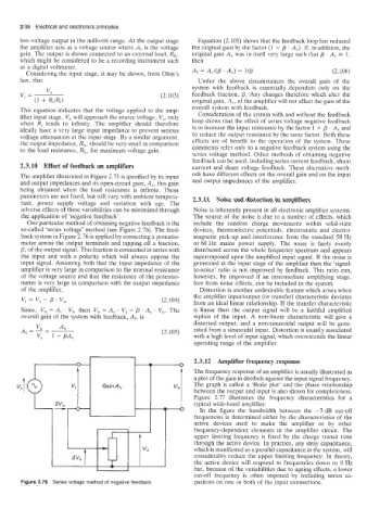
One particular method of obtaining negative feedback is the include the random charge movements within solid-state
so-called 'series voltage' method (see Figure 2.76). The feed- devices, thermoelectric potentials, electrostatic and electro-
back system in Figure 2.76 is applied by connecting a potentio- magnetic pick-up and interference from the standard 50 Hz
meter across the output terminals and tapping off a fraction, or 60 Hz mains power supply. The noise is fairly evenly
p, of the output signal. This fraction is connected in series with distributed across the whole frequency spectrum and appears
the input and with a polarity which will always oppose the superimposed upon the amplified input signal. If the noise is
input signal. Assuming both that the input impedance of the generated at the input stage of the amplifier then the 'signal-
amplifier is very large in comparison to the internal resistance to-noise' ratio is not improved by feedback. This ratio can,
of the voltage source and that the resistance of the potentio- however, be improved if an intermediate amplifying stage,
meter is very large in comparison with the output impedance free from noise effects, can be included in the system.
of the amplifier, Distortion is another undesirable feature which arises when
VI = v, - p . v, (2.104) the amplifier input/output (or transfer) characteristic deviates
from an ideal linear relationship. If the transfer characteristic
Since, V, = A, . Vi, then V, = A, . V, - p . A, . V,. The is linear then the output signal will be a faithful amplified
overall gain of the system with feedback, Af, is replica of the input. A non-linear characteristic will give a
distorted output, and a non-sinusoidal output will be gene-
-
rated from a sinusoidal input. Distortion is usually associated
(2.105)
with a high level of input signal, which overextends the linear
operating range of the amplifier.
A 2.3.12 Amplifier frequency response
The frequency response of an amplifier is usually illustrated as
a plot of the gain in decibels against the input signal frequency.
Gain A, VO The graph is called a 'Bode plot' and the phase relationship
between the output and input is also shown for completeness.
Figure 2.77 illustrates the frequency characteristics for a
typical wide-band amplifier.
In the figure the bandwidth between the -3 dB cut-off
frequencies is determined either by the characteristics of the
active devices used to make the amplifier or by other
frequency-dependent elements in the amplifier circuit. The
ILIt
upper limiting frequency is fixed by the charge transit time
I XtU lvo which is manifested as a parallel capacitance in the system, will
1
through the active device. In practice, any stray capacitance,
considerably reduce the upper limiting frequency. In theory,
the active device will respond to frequencies down to 0 Hz
but, because of the variabilities due to ageing effects, a lower
cut-off frequency is often imposed by including series ca-
Figure 2.76 Series voltage method of negative feedback pacitors on one or both of the input connections.