
Page 100 - Mechanical Engineers Reference Book
P. 100
Analogue and digital electronics theory 2/41
or
(2.1 12)
If the resistances used in the circuit are all of equal value.
the output voltage will be equivalent to the summation of all
the input voltages and with a reversed sign. Subtraction of any
of the voltages can be performed by reversing its polarity. i.e.
Sy first passing the voltage through a unity gain inverting
amplifier before it is passed on to the summing amplifier.
2 3.I4.5 Integrating amplifier
The integrating amplifier uses a capacitor, as opposed to a
resistor, in the feedback loop (see Figure 2.83). The voltage
across tlhe capacitor is
R1
l/C 1’ tzdt v, = E2 [V 2- V,I
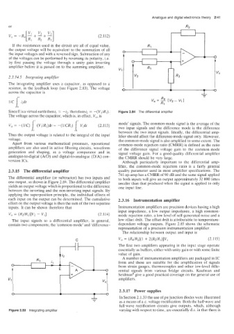
SinceEiisavirtualearththenz, = -iz. thereforeiz = -(VI/RI). Figure 2.84 The differential amplifier
The voltage across the capacitor, which is. in effect, Vo, is
J(I two input signals and the difference mode is the difference
Vo = -(l/C) (Vl/R,)dt = -(l/CRI) iTi Vldt (2.113) mode’ signals. The common-mode signal is the average of the
Thus thi- output voltage is related to the integral of the input between the two input signals. Ideally, the differential amp-
lifier should affect the difference-mode signal only. However:
voltage. the common-mode signal is also amplified to some extent. The
Apart from various mathematical processes, operational common-mode rejection ratio (CMRR) is defined as the ratio
amplifiers are also used in active filtering circuits, waveform of the difference signal voltage gain to the common-mode
generation and shaping, as a voltage comparator and in signal voltage gain. For a good-quality differential amplifier
analogue-to-digital (AID) and digital-to-analogue (DIA) con- the CMRR should be very large.
version ICs. Although particularly important to the differential amp-
lifier, the common-mode rejection ratio is a fairly general
2.3.15 The differential amplifier quality parameter used in most amplifier specifications. The
741 op-amp has a CMRR of 90 dB and the same signal applied
The differential amplifier (or subtractor) has two inputs and to both inputs will give an output approximately 32 000 times
one output. as shown in Figure 2.84. The differential amplifier smaller than that produced when the signal is applied to only
yields an output voltage which is proportional to the difference one input line.
between the inverting and the non-inverting input signals. By
applying the superposition principle, the individual effects of
each input on the output can be determined. The cumulative 2.3.16 Instrumentation amplifier
effect on the output voltage is then the sum of the two separate
inputs. It can be shown therefore that Instrumentation amplifiers are precision devices having a high
input impedance, a low output impedance, a high common-
vo = (RZ/RI)[VZ - V,] (2.114) mode rejection ratio. a low level of self-generated noise and a
The input signals to a differential amplifier, in general, low offset drift. The offset drift is attributable to temperature-
contain two components; the ‘commonmode’ and ‘difference- dependent voltage outputs. Figure 2.85 shows the schematic
representation of a precision instrumentation amplifier.
The relationship between output and input is
C (2.115)
The first two amplifiers appearing in the input stage operate
essentially as buffers, either with unity gain or with some finite
value of gain.
A number of instrumentation amplifiers are packaged in IC
form and these are suitable for the amplification of signals
from strain gauges, thermocouples and other low-level diffe-
rential signals from various bridge circuits. Kaufman and
Seidman8 give a good practical coverage on the general use of
v1 amplifiers.
2.3.17 Power supplies
In Section 2.1.33 the use ofpn junction diodes were illustrated
as a means of a.c. voltage rectification. Both the half-wave and
full-wave rectification circuits give outputs, which, although
Figure 2.83 Integrating amplifier varying with respect to time, are essentially d.c. in that there is