
Page 95 - Mechanical Engineers Reference Book
P. 95
2/36 Electrical and electronics principles
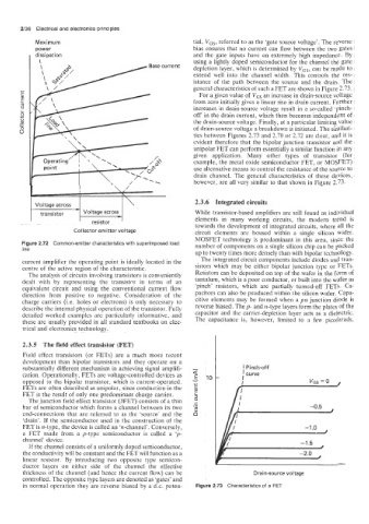
Maximum tial, VGs, referred to as the ‘gate source voltage’. The reverse
power bias ensures that no current can flow between the two gates
dissipation and the gate inputs have an extremely high impedance. By
using a lightly doped semiconductor for the channel the gate
depletion layer, which is determined by VGS, can be made to
extend well into the channel width. This controls the res-
istance of the path between the source and the drain. The
general characteristics of such a FET are shown in Figure 2.73.
For a given value of VGS an increase in drain-source voltage
from zero initially gives a linear rise in drain current. Further
increases in drain-source voltage result in a so-called ‘pinch-
off‘ in the drain current, which then becomes independent of
the drain-source voltage. Finally, at a particular limiting value
of drain-source voltage a breakdown is initiated. The similari-
ties between Figures 2.73 and 2.70 or 2.72 are clear, and it is
evident therefore that the bipolar junction transistor and the
unipolar FET can perform essentially a similar function in any
,’+ given application. Many other types of transistor (for
Operating example, the metal oxide semiconductor FET, or MOSFET)
point ~ ‘\ \ 4X0 use alternative means to control the resistance of the source to
drain channel. The general characteristics of these devices,
however, are all very similar to that shown in Figure 2.73.
2.3.6 Integrated circuits
While transistor-based amplifiers are still found as individual
elements in many working circuits, the modern trend is
resistor towards the development of integrated circuits, where all the
Collector-emitter voltage circuit elements are housed within a single silicon wafer.
MOSFET technology is predominant in this area, since the
Figure 2.72 Common-emitter characteristics with superimposed load number of components on a single silicon chip can be packed
line
up to twenty times more densely than with bipolar technology.
current amplifier the operating point is ideally located in the The integrated circuit components include diodes and tran-
centre of the active region of the characteristic. sistors which may be either bipolar junction type or FETs.
The analysis of circuits involving transistors is conveniently Resistors can be deposited on top of the wafer in the form of
dealt with by representing the transistnr in terms of an tantalum, which is a poor conductor, or built into the wafer as
equivalent circuit and using the conventional current flow ‘pinch’ resistors, which are partially turned-off FETs. Ca-
direction from positive to negative. Consideration of the pacitors can also be produced within the silicon wafer. Capa-
charge carriers (i.e. holes or electrons) is only necessary to citive elements may be formed when a pn junction diode is
describe the internal physical operation of the transistor. Fully reverse biased. Thep- and n-type layers form the plates of the
detailed worked examples are particularly informative, and capacitor and the carrier-depletion layer acts as a dielectric.
these are usually provided in all standard textbooks on elec- The capacitance is, however, limited to a few picofarads.
trical and electronics technology.
2.3.5 The field effect transistor (FET)
Field effect transistors (or FETs) are a much more recent
development than bipolar transistors and they operate on a
substantially different mechanism in achieving signal amplifi- I Pinch-off
cation. Operationally, FETs are voltage-controlled devices as Q I curve
opposed to the bipolar transistor, which is current-operated. c I VGS = 0
FETs are often described as unipolar, since conduction in the
FET is the result of only one predominant charge carrier.
The junction field effect transistor (JFET) consists of a thin .-
bar of semiconductor which forms a channel between its two E -0.5
end-connections that are referred to as the ‘source’ and the 0
‘drain’. If the semiconductor used in the construction of the
FET is n-type, the device is called an %channel’. Conversely, -5
a FET made from a p-type semiconductor is called a ‘p-
channel’ device.
If the channel consists of a uniformly doped semiconductor,
the conductivity will be constant and the FET will function as a / -2.0
linear resistor. By introducing two opposite type semicon-
ductor layers on either side of the channel the effective
thickness of the channel (and hence the current flow) can be Drain-source voltage
controlled. The opposite type layers are denoted as ‘gates’ and
in normal operation they are reverse biased by a d.c. poten- Figure 2.73 Characteristics of a FET