
Page 92 - Mechanical Engineers Reference Book
P. 92
Analogue and digital electronics theory 2/33
P 2.3 Analogue and digital electronics theory
2.3.1 The bipolar (or junction) transistor
The term ‘transistor’, derived from ‘transfer resistor‘, des-
cribes a device which can transfer a current from a low-
resistance circuit to a high-resistance one with little change in
current during the process. The junction transistor consists of
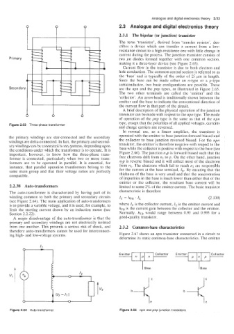
Primary two pn diodes formed together with one common section,
making it a three-layer device (see Figure 2.65).
Current flow in the transistor is due to both electron and
hole conduction. The common central section is referred to as
the ‘base’ and is typically of the order of 25 pm in length.
Since the base can be made either an n-type or a p-type
semiconductor, two basic configurations are possible. These
Secondary are the npn and the pnp types, as illustrated in Figure 2.65.
The two other terminals are called the ‘emitter’ and the
‘collector’. An arrowhead is traditionally shown between the
emitter and the base to indicate the conventional direction of
the current flow in that part of the circuit.
A brief description of the physical operation of the junction
transistor can be made with respect to the npn type. The mode
of operation of the pnp type is the same as that of the npn
Figure 2..63 Three-phase transformer type, except that the polarities of all applied voltages, currents
and charge carriers are reversed.
In normal use, as a linear amplifier, the transistor is
the primary windings are star-connected and the secondary operated with the emitter to base junction forward biased and
the collector to base junction reversed biased. For the npn
windings are delta-connected. In fact, the primary and second-
ary windings can be connected in any pattern, depending upon transistor, the emitter is therefore negative with respect to the
the conditions under which the transformer is to operate. It is base while the collector is positive with respect to the base (see
important, however, to know how the three-phase trans- Figure 2.66). The junction np is forward biased such that the
former is connected, particularly when two or more trans- free electrons drift from n1 top. On the other hand, junction
formers are to be operated in parallel. It is essential, for ng is reverse biased and it will collect most of the electrons
instance, that parallel operation transformers belong to the from nl. The electrons which fail to reach n2 are responsible
same main group and that their voltage ratios are perfectly for the current at the base terminal, 2,. By ensuring that the
compatible. thickness of the base is very small and that the concentration
of impurities in the base is much lower than either that of the
emitter or the collector, the resultant base current will be
2.2.38 Auto-transformers limited to some 2% of the emitter current. The basic transistor
characteristic is therefore
The auto-transformer is characterized by having part of its
winding common to both the primary and secondary circuits = hFB ’ ZE (2.100)
(see Figure 2.64). The main application of auto-transformers
is to provide a variable voltage, and it is used, for example, to where 2, is the collector current, 2, is the emitter current and
limit the starting current drawn by an induction motor (see hFB is the current gain between the collector and the emitter.
Section 2.2.22). Normally. hFB would range between 0.95 and 0.995 for a
A major disadvantage of the auto-transformer is that the good-quality transistor.
primary and secondary windings are not eiectrically isolated
from one another. This presents a serious risk of shock, and 2.3.2 Common-base characteristics
therefore auto-transformers cannot be used for interconnect-
ing high- and low-voltage systems. Figure 2.67 shows an npn transistor connected in a circuit to
determine its static common-base characteristics. The emitter
Emitter Collector Emitter Collector
Vl t I Base I Base
Figure 2.64 Auto-transformer Figure 2.65 npn and pnp junction transistors