
Page 94 - Mechanical Engineers Reference Book
P. 94
Analogue and digital electronics theory 2/35
If. due to some temperature effect, hFB undergoes a minor
change to, say, 0.96. the new value of hFE becomes 24. It is
clear therefore that the common-emitter gain, hFE, is much
more sensitive to small-order effects than the common-base
gain, hFB.
For a pnp transistor the characteristics of the common-
emitter circuit are the same, except that the polarity of all
voltages and currents are again in reverse order to that shown
in Figure 2.69.
2.3.4 The transistor in a circuit
In most practical applications transistors are operated in the
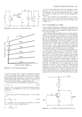
Figure 2.69 npn transistor in common emitter circuit common-emitter mode where the emitter terminal forms the
common connection between the input and output sections of
the circuit (see Figure 2.71).
The transistor collector characteristics are shown again in
Figure 2.72. The load line for the resistor, Rc, is superimposed
and the operating point is given by the intersection of the load
line with the collector characteristic. The operating point will
therefore be dependent on the base current, since this controls
the collector characteristic. Also shown in Figure 2.72 is the
5 maximum power dissipation curve (broken line), which repre-
a
- collector-emitter voltage. The maximum power dissipation
sents the locus of the product of collector current and
E
e4 curve represents a physical limitation and the operating point
must be constrained to lie below the curve at all times.
As the base current is reduced the operating point moves
$ I down the load line. When I, reaches zero the collector current
will be minimized and the transistor is said to be ‘cut-off‘.
L
0
4-
Alternatively, as the base current is increased the operating
-
0 2 point moves up the load line and eventually reaches a maxi-
0 mum value at which the transistor is said to be ’bottomed’, or
1 ‘saturated’. When saturated, the collector-emitter voltage is at
a minimum of about 0.1-0.2 V and the collector current is a
maximum. The two extremes between cut-off and saturation
represent a very high and a very low impedance state of the
transistor, respectively. These extremes have great practical
Collector-emitter voltage, VcE
application to rapid, low-power switching, and transistors
operating between cut-off and saturation are frequently used
Figure 2.710 Common-emitter characteristics
in digital electronics circuitry. The low-impedance state repre-
sents a switch closed (or on) and the high-impedance state
represents the switch open (or off). When operating as a linear
exceeds the so-called ‘knee’ voltage the characteristic assumes
a linear relationship. The gradient of the linear region is
generally much higher than that for the common-base configu-
ration and the collector impedance is therefore lower than that
for the common-base circuit. When the base current is zero
the collector current still has a positive finite value.
The common-emitter characteristic is generally written as
IC = hFE . I, (2.101)
where hFE is the current gain between the collector and base.
Application of Kirchhoffs first law to the common-emitter
circuit gives
I, = 1, i- I,
Using equation (2.100) and eliminating I,, it can be shown
that Output
I VCE
(2.102) Input
For a transistor with a steady-state current gain in common
base of 0.95 the common-emitter gain is
OV
0.95
hFE = ~ = 19
1 - 0.95 Figure 2.71 npn transistor in a practical common-emitter circuit