
Page 251 - Mechanical Engineers' Handbook (Volume 2)
P. 251
240 Digital Integrated Circuits: A Practical Application
2 FIELD-PROGRAMMABLE GATE ARRAYS
Field programmable gate array technology permits the design of many different complex
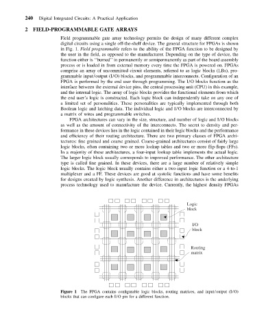
digital circuits using a single off-the-shelf device. The general structure for FPGAs is shown
in Fig. 1. Field programmable refers to the ability of the FPGA function to be designed by
the user in the field, as opposed to the manufacturer. Depending on the type of device, the
function either is ‘‘burned’’ in permanently or semipermanently as part of the board assembly
process or is loaded in from external memory every time the FPGA is powered on. FPGAs
comprise an array of uncommitted circuit elements, referred to as logic blocks (LBs), pro-
grammable input/output (I/O) blocks, and programmable interconnects. Configuration of an
FPGA is performed by the end user through programming. The I/O blocks function as the
interface between the external device pins, the central processing unit (CPU) in this example,
and the internal logic. The array of logic blocks provides the functional elements from which
the end user’s logic is constructed. Each logic block can independently take on any one of
a limited set of personalities. These personalities are typically implemented through both
Boolean logic and latching data. The individual logic and I/O blocks are interconnected by
a matrix of wires and programmable switches.
FPGA architectures can vary in the size, structure, and number of logic and I/O blocks
as well as the amount of connectivity of the interconnects. The secret to density and per-
formance in these devices lies in the logic contained in their logic blocks and the performance
and efficiency of their routing architecture. There are two primary classes of FPGA archi-
tectures: fine grained and coarse grained. Coarse-grained architectures consist of fairly large
logic blocks, often containing two or more lookup tables and two or more flip-flops (FFs).
In a majority of these architectures, a four-input lookup table implements the actual logic.
The larger logic block usually corresponds to improved performance. The other architecture
type is called fine grained. In these devices, there are a large number of relatively simple
logic blocks. The logic block usually contains either a two-input logic function or a 4-to-1
multiplexer and a FF. These devices are good at systolic functions and have some benefits
for designs created by logic synthesis. Another difference in architectures is the underlying
process technology used to manufacture the device. Currently, the highest density FPGAs
Logic
block
I/O
block
Routing
matrix
Figure 1 The FPGA contains configurable logic blocks, routing matrices, and input/output (I/O)
blocks that can configure each I/O pin for a different function.