
Page 253 - Mechanical Engineers' Handbook (Volume 2)
P. 253
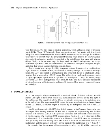
242   Digital Integrated Circuits: A Practical Application


                                                                C out

                                                                            D
                                                                LUT

                                                                            D
                                                                LUT

                                                                C in


                                     Figure 2 General logic block with two-input logic and D-type FFs.


                          uses three stages. The first stage is function generation, which utilizes an array of program-
                          mable LUTs. These LUTs typically have between three and five inputs, with four inputs
                          being cited as the best compromise between LUT access time and the average desired func-
                          tion delay. The second stage, the programmable routing stage, follows the function gener-
                                  1
                          ators and allows function results to be supplied to the logic block’s final stage with minimal
                          delays. Finally, in the memory stage, the logic block uses D FFs to implement bit storage
                          within the logic block. The FFs are beneficial for distributed storage in configured designs,
                          including their use as registers between pipeline stages.
                             Logic blocks have enough flexibility to operate in three distinct modes: combinational
                          logic, arithmetic or ripple modes, and dedicated memory storage. In combinational logic
                          mode, the LUTs are loaded at configuration time with truth tables to implement a logic
                          function that is independent of LUT inputs. The arithmetic or ripple mode uses carry gates
                          to rapidly propagate signals from a logic block to its neighbors. Lastly, the memory stage
                          allows the LUT to be configured as RAM or ROM units. This mode increases the amount
                          of internal memory within the device and is useful for embedding memory elements through-
                          out a design.


           4  LOOKUP TABLES

                          A LUT of a regular, single-context FPGA consists of a bank of SRAM cells and a multi-
                          plexer. The depth of the SRAM cell is one, and it should be as wide as the data input of
                          the multiplexer. The output bits of the SRAM are directly connected to the data input pins
                          of the multiplexer. The inputs to the LUT control the select signals of the multiplexer. Based
                          on the LUT inputs, an SRAM output is selected by the multiplexer and sent to the LUT
                          output.
                             A K-input lookup table (K-LUT) is a digital memory with K address lines and a one-
                          bit output. This memory contains 2K bits and is capable of implementing any Boolean
                          function of K variables. A LUT of K inputs can implement 22K different Boolean functions.
                          A simple example of a two-input LUT implementing a function ƒ   a   b  is shown in Fig.
                          3, where the LUT is described in terms of a multiplexer. In the LUT, there are two address
                          lines (a and b) and four memory cells. The inputs to the LUT are the select lines of the
                          multiplexer, and the memory cells serve as the inputs to the multiplexer. If a   0 and b
                          1, for example, then the memory cell corresponding to select line 01 will be connected to