Page 183 -
P. 183
5.2 Theoretical Analysis  173
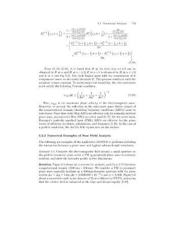
                                                      1
                                                  σ(i+ ,j,k)∆t                    ∆t
                                               1 −    2
                                                                                  1
                                                       1
                                                   2ε(i+ ,j,k)                 ε(i+ ,j,k)
                               n+1        1            2      n        1          2
                             E z   i, j, k +  =              E z  i, j, k +  +
                                                      1
                                          2       σ(i+ ,j,k)∆t         2       σ(i+ ,j,k)∆t
                                                                                   1
                                               1+     2                     1+     2
                                                       1
                                                   2ε(i+ ,j,k)                  2ε(i+ ,j,k)
                                                                                    1
                                                       2                            2
                                                    n+  1    1    1     n+  1    1     1

                                                  H y  2  i + ,j,k +  − H y  2  i − ,j,k +
                                                           2      2             2      2
                                               ×
                                                                    ∆x
                                                      n+  1    1     1     n+  1    1     1
                                                    H x  2  i, j − ,k +  2  − H x  2  i, j + ,k +  2
                                                                                    2
                                                               2
                                                   +                                         .
                                                                       ∆y
                                                                                          (5.18)
                                From (5.13)–(5.18), it is found that H at the time step n+1/2 can be
                            obtained by E at n and H at n − 1/2,E at n + 1 is obtained by H at n +1/2
                            and E at n (see Fig. 5.3). The cycle begins again with the computation of E
                            components based on the newly obtained H. This process continues until the
                            solutions remain constant. To avoid numerical instability, the time increment
                            must satisfy the followingCourant condition:
                                                                            1
                                                         1      1     1     2
                                                                           −
                                             v max ∆t ≤    2  +  2  +   2    .            (5.19)
                                                        ∆x     ∆y    ∆z
                               Here, v max is the maximum phase velocity of the electromagnetic wave.
                            Moreover, to prevent the reflection at the outermost space–lattice planes of
                            the computational domain, absorbingboundary conditions (ABCs) must be
                            introduced. Since first-order Mur ABCs are effective only for normally incident
                            plane wave, second-order Mur ABCs are often used [5.17]. On the other hand,
                            Berenger’s perfectly matched layer (PML) ABCs are effective for the plane
                            waves of arbitrary incidence, polarization, and frequency [5.18]. In the case of
                            a perfect conductor, the electric field equals zero on the surface.
                            5.2.2 Numerical Examples of Near Field Analysis
                            The followingare examples of the application of FDTD to problems including
                            the interaction between a plane wave and typical subwavelength structures.

                            Example 5.1. Compute the electromagnetic field around a small aperture on
                            the perfect conductor plane when a TM (p-polarized) plane wave is normally
                            incident, and show the intensity profile in two dimensions.
                            Solution. Figure 5.5 shows (a) a process for analysis, and (b) a 2-D Cartesian
                            computational domain (1500 nm × 500 nm). We consider a TM (p-polarized)
                            plane wave normally incident on a 100-nm-diameter aperture with the para-
                            meters ∆x =∆y =1 nm, ∆t =2.3586769 × 10 −19  sand n =3, 000. Figure 5.6
                            shows a numerical result in the domain of 75 nm×500 nm by FDTD, indicating
                            that the electric field is enhanced at the edge and decays rapidly [5.19].

