
Page 188 -
P. 188
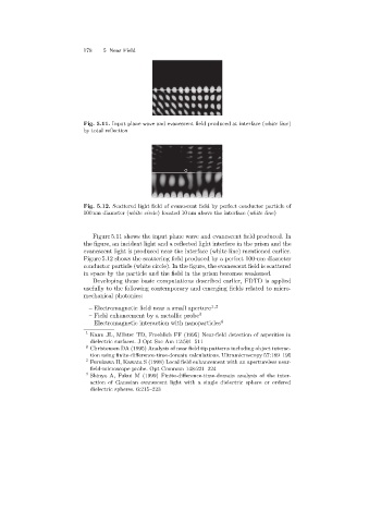
178   5 Near Field


                            Fig. 5.11. Input plane wave and evanescent field produced at interface (white line)
                            by total reflection


                            Fig. 5.12. Scattered light field of evanescent field by perfect conductor particle of
                            100 nm diameter (white circle)located 10 nm above the interface (white line)


                               Figure 5.11 shows the input plane wave and evanescent field produced. In
                            the figure, an incident light and a reflected light interfere in the prism and the
                            evanescent light is produced near the interface (white line) mentioned earlier.
                            Figure 5.12 shows the scattering field produced by a perfect 100-nm diameter
                            conductor particle (white circle). In the figure, the evanescent field is scattered
                            in space by the particle and the field in the prism becomes weakened.
                               Developingthese basic computations described earlier, FDTD is applied
                            usefully to the followingcontemporary and emergingfields related to micro-
                            mechanical photonics:

                              – Electromagnetic field near a small aperture 1,2
                              – Field enhancement by a metallic probe 3
                              – Electromagnetic interaction with nanoparticles 4

                             1
                              Kann JL, Milster TD, Froehlich FF (1995)Near-field detection of asperities in
                              dielectric surfaces. J Opt Soc Am 12:501–511
                             2  Christensen DA (1995)Analysis of near field tip patterns including object interac-
                              tion using finite-difference-time-domain calculations. Ultramicroscopy 57:189–195
                             3  Furukawa H, Kawata S (1998)Local field enhancement with an apertureless near-
                              field-microscope probe. Opt Commun 148:221–224
                             4
                              Shinya A, Fukui M (1999)Finite-difference-time-domain analysis of the inter-
                              action of Gaussian evanescent light with a single dielectric sphere or ordered
                              dielectric spheres. 6:215–223