
Page 191 - Microsensors, MEMS and Smart Devices - Gardner Varadhan and Awadelkarim
P. 191
ADHESION PROBLEMS IN SURFACE MICROMACHINING 171
Unreleased
polysilicon Holes Silicon dioxide Silicon dioxide Polymer columns
microstractureV S_ t \
(a)
Photoresist Oxide undercut
_ , Aluminum Free
Parylene / \ polysilicon \Oxygen plasma column removal
microstructure^
(c) (f)
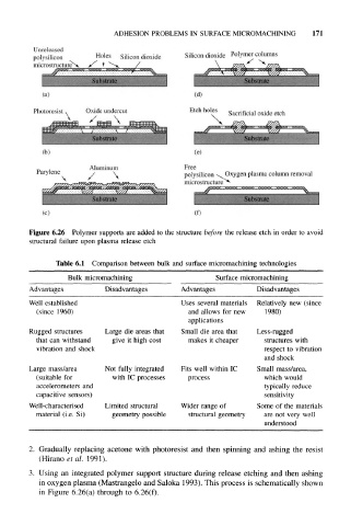
Figure 6.26 Polymer supports are added to the structure before the release etch in order to avoid
structural failure upon plasma release etch
Table 6.1 Comparison between bulk and surface micromachining technologies
Bulk micromachining Surface micromachining
Advantages Disadvantages Advantages Disadvantages
Well established Uses several materials Relatively new (since
(since 1960) and allows for new 1980)
applications
Rugged structures Large die areas that Small die area that Less-rugged
that can withstand give it high cost makes it cheaper structures with
vibration and shock respect to vibration
and shock
Large mass/area Not fully integrated Fits well within 1C Small mass/area,
(suitable for with 1C processes process which would
accelerometers and typically reduce
capacitive sensors) sensitivity
Well-characterised Limited structural Wider range of Some of the materials
material (i.e. Si) geometry possible structural geometry are not very well
understood
2. Gradually replacing acetone with photoresist and then spinning and ashing the resist
(Hirano et al. 1991).
3. Using an integrated polymer support structure during release etching and then ashing
in oxygen plasma (Mastrangelo and Saloka 1993). This process is schematically shown
in Figure 6.26(a) through to 6.26(f).