
Page 190 - Microsensors, MEMS and Smart Devices - Gardner Varadhan and Awadelkarim
P. 190
170 SILICON MICROMACHINING: SURFACE
A final timed etch of sacrificial PSG fully exposes the overhanging poly-Si micro
to the substrate (Figure 6.23(e)).I
gripper by removing PSG from top and bottom. All poly-Si conducting lines have a
I PSG layer left underneath them, which anchors them
6.7 ADHESION PROBLEMS IN SURFACE
MICROMACHINING
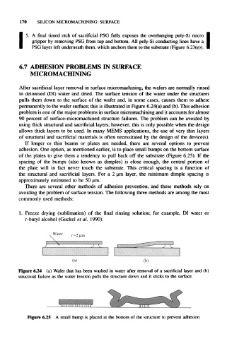
After sacrificial layer removal in surface micromachining, the wafers are normally rinsed
in deionised (DI) water and dried. The surface tension of the water under the structures
pulls them down to the surface of the wafer and, in some cases, causes them to adhere
permanently to the wafer surface; this is illustrated in Figure 6.24(a) and (b). This adhesion
problem is one of the major problems in surface micromachining and it accounts for almost
90 percent of surface-micromachined structure failures. The problem can be avoided by
using thick structural and sacrificial layers; however, this is only possible when the design
allows thick layers to be used. In many MEMS applications, the use of very thin layers
of structural and sacrificial materials is often necessitated by the design of the device(s).
If longer or thin beams or plates are needed, there are several options to prevent
adhesion. One option, as mentioned earlier, is to place small bumps on the bottom surface
of the plates to give them a tendency to pull back off the substrate (Figure 6.25). If the
spacing of the bumps (also known as dimples) is close enough, the central portion of
the plate will in fact never touch the substrate. This critical spacing is a function of
the structural and sacrificial layers. For a 2 um layer, the minimum dimple spacing is
approximately estimated to be 50 um.
There are several other methods of adhesion prevention, and these methods rely on
avoiding the problem of surface tension. The following three methods are among the most
commonly used methods:
1. Freeze drying (sublimation) of the final rinsing solution; for example, DI water or
/-butyl alcohol (Guckel et al. 1990).
Water , =2 um
Figure 6.24 (a) Wafer that has been washed in water after removal of a sacrificial layer and (b)
structural failure as the water tension pulls the structure down and it sticks to the surface
Figure 6.25 A small bump is placed at the bottom of the structure to prevent adhesion