
Page 185 - Microsensors, MEMS and Smart Devices - Gardner Varadhan and Awadelkarim
P. 185
165
3. About 600 nm of borophosphosilicate glass (BPSG) is deposited at 400 °C. BPSG
serves as an interlevel dielectric between the poly-Si gate and metal and is also a
sacrificial layer that sets the gap. The BPSG is then patterned and plasma-etched using
CF4 that is timed to stop at Si3N4 because CF4 also etches Si 3N 4 (Figure 6.18(c)).
4. A 1 um layer of poly-Si is deposited by LPCVD at 625 °C, doped with phosphorus
using a POC1 3 source at 925 °C, and the phosphorus glass wet-etched. A front-coat
resist is applied and a backside poly-Si plasma etch is performed using SFf, stopping
on the BPSG layer. The poly-Si layer serves as the top plate of the air gap capacitor
and is patterned or plasma-etched in CC1 4 (Figure 6, 1 8(d)).
5. After etching, the process returns to a normal back-end MOS process that consists
of patterning or etching contact cuts into the BPSG, followed by a sputter deposition
of aluminum (with 1 percent Si) to a thickness of 1.1 um. The metal is patterned,
plasma-etched, and sintered to complete the front-side processing (Figure 6.18(e)).
The contact to the n + bottom plate is made via n + diffusion channels contacted by
the metal that surrounds the diaphragm. Contact to the poly-Si is made directly via
metal on top of a tab that protrudes from the square structure.
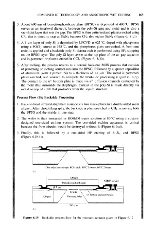
Process Flow (B): Backside Processing
1 . Back-to-front infrared alignment is made via two mask-plates in a double-sided mask
aligner. After photolithography, the backside is plasma-etched in CH4, removing both
the BPSG and the nitride in one step.
2. The wafer is then immersed in KOH/DI water solution at 80 °C using a custom-
designed one-sided etching system. The one-sided etching apparatus is critical
because the front circuits would be destroyed without it (Figure 6.19(a)).
3. Finally, this is followed by a one-sided HF etching of and BPSG
(Figure 6.19(b)).
One-sided anisotropic KOH etch: 80°C 6 hours, 60°C 2 hours
100 u
50 um \ \
\ n+ bottom capacitor plate
500 um Pressure inlet x
760 um
Figure 6.19 Backside process flow for the resonant actuator given in Figure 6.17