
Page 182 - Microsensors, MEMS and Smart Devices - Gardner Varadhan and Awadelkarim
P. 182
162 SILICON MICROMACHINING: SURFACE
Thermally grown
silicon dioxide
(2.5 Jim)
(a)
Phosphorus-doped
LPCVD polysilicon
CVD silicon nitride
(b) (250 nm)
Nickel
(100 nm)
(c)
Fixed Suspended Silicon dioxide in
oxidation machining
electrode electrode
I • I
(d)
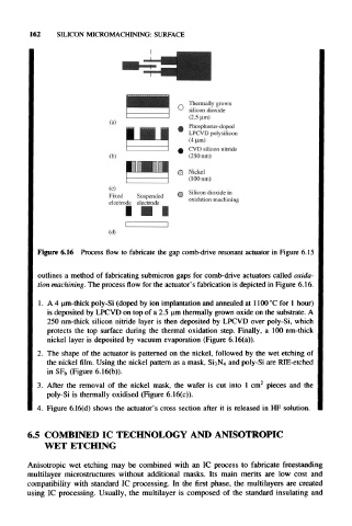
Figure 6.16 Process flow to fabricate the gap comb-drive resonant actuator in Figure 6.15
outlines a method of fabricating submicron gaps for comb-drive actuators called oxida-
tion machining. The process flow for the actuator's fabrication is depicted in Figure 6.16.
1. A 4 um-thick poly-Si (doped by ion implantation and annealed at 1100°C for 1 hour)
is deposited by LPCVD on top of a 2.5 um thermally grown oxide on the substrate. A
250 nm-thick silicon nitride layer is then deposited by LPCVD over poly-Si, which
protects the top surface during the thermal oxidation step. Finally, a 100 nm-thick
nickel layer is deposited by vacuum evaporation (Figure 6.16(a)).
2. The shape of the actuator is patterned on the nickel, followed by the wet etching of
and poly-Si are RIE-etched
the nickel film. Using the nickel pattern as a mask, Si3N 4
in SF 6 (Figure 6.16(b)).
3. After the removal of the nickel mask, the wafer is cut into 1 cm 2 pieces and the
poly-Si is thermally oxidised (Figure 6.16(c)).
4. Figure 6.16(d) shows the actuator's cross section after it is released in HF solution.
6.5 COMBINED 1C TECHNOLOGY AND ANISOTROPIC
WET ETCHING
Anisotropic wet etching may be combined with an 1C process to fabricate freestanding
multilayer microstructures without additional masks. Its main merits are low cost and
compatibility with standard 1C processing. In the first phase, the multilayers are created
using 1C processing. Usually, the multilayer is composed of the standard insulating and