
Page 178 - Microsensors, MEMS and Smart Devices - Gardner Varadhan and Awadelkarim
P. 178
158 SILICON MICROMACHINING: SURFACE
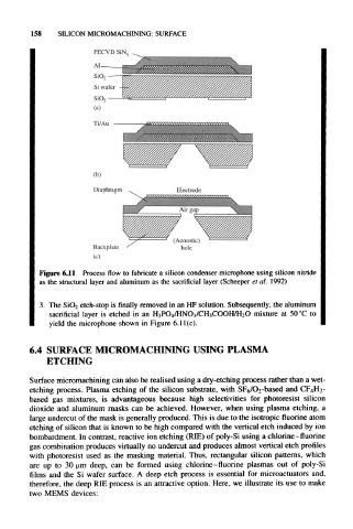
(b)
Diaphragm Electrode
(Acoustic)
Backplate hole
(c)
Figure 6.11 Process flow to fabricate a silicon condenser microphone using silicon nitride
as the structural layer and aluminum as the sacrificial layer (Scheeper et al. 1992)
3. The SiO 2 etch-stop is finally removed in an HF solution. Subsequently, the aluminum
sacrificial layer is etched in an H 3PO 4/HNO 3/CH 3COOH/H 2O mixture at 50 °C to
yield the microphone shown in Figure 6.11 (c).
6.4 SURFACE MICROMACHINING USING PLASMA
ETCHING
Surface micromachining can also be realised using a dry-etching process rather than a wet-
etching process. Plasma etching of the silicon substrate, with SFe/CVbased and CF 4H2-
based gas mixtures, is advantageous because high selectivities for photoresist silicon
dioxide and aluminum masks can be achieved. However, when using plasma etching, a
large undercut of the mask is generally produced. This is due to the isotropic fluorine atom
etching of silicon that is known to be high compared with the vertical etch induced by ion
bombardment. In contrast, reactive ion etching (REE) of poly-Si using a chlorine-fluorine
gas combination produces virtually no undercut and produces almost vertical etch profiles
with photoresist used as the masking material. Thus, rectangular silicon patterns, which
are up to 30 urn deep, can be formed using chlorine-fluorine plasmas out of poly-Si
films and the Si wafer surface. A deep etch process is essential for microactuators and,
therefore, the deep RIE process is an attractive option. Here, we illustrate its use to make
two MEMS devices: