
Page 183 - Microsensors, MEMS and Smart Devices - Gardner Varadhan and Awadelkarim
P. 183
COMBINED 1C TECHNOLOGY AND ANISOTROPIC WET ETCHING 163
passivating dielectric films, poly-Si layers, and metal layers. The poly-Si and metal layers
constitute the active layers and are usually sandwiched between the dielectric films that
are necessary for electrical insulation and component passivation. By special design,
windows are opened around the multilayer structures for removal of all dielectric layers,
thus exposing the silicon surface underneath.
In the second so-called postprocessing phase, the wafers are immersed in anisotropic
silicon etchants. Thus, the exposed silicon surface around the multilayer structure is
removed, and by under-etching, the microstructures finally become freestanding. Because
the active layers are completely contained within the dielectric layers, they are protected
against the silicon-etching process.
An alternative approach is to etch anisotropically only the backside of the wafer, that
is, use a single-sided etching bath. This technique may be used to make certain structures
but tends to be a more time-consuming, and therefore, a more costly process. A worked
example is now provided.
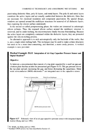
Worked Example E6.8: Integration of Air Gap Capacitor Pressure Sensor and
13
Digital Readout
Objective:
To fabricate a microstructure that consists of a top plate separated by a small air gap and
a bottom plate that has an inlet for pressurised gas (Figure 6.17). The gas pressure moves
the top plate upward, increasing the gap, and hence decreasing the capacitance. Metal
14
oxide semiconductor (MOS) electronics are integrated next to the capacitive sensor.
Contact to bottom plate Polysilicon diaphragm
Figure 6.17 Schematic view of an air gap capacitive pressure sensor with integrated digital
readout (Kung and Lee 1992)
13
For details, see Kung and Lee (1992).
14
Standard CMOS process has been described in Section 4.3.