
Page 184 - Microsensors, MEMS and Smart Devices - Gardner Varadhan and Awadelkarim
P. 184
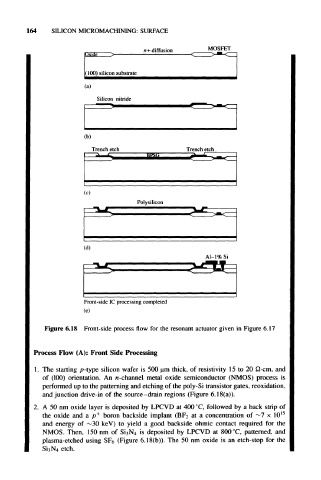
164    SILICON  MICROMACHINING:  SURFACE

                                      n+  diffusion    MOSFET


                     (100)  silicon  substrate
                     (a)
                         Silicon  nitride


                     (b)
                       Trench etch               Trench etch


                     (c)
                                    Polysilicon


                     (d)


                     Front-side 1C processing completed
                     (e)

          Figure 6.18  Front-side process flow for the resonant  actuator  given  in Figure 6.17


       Process Flow  (A):  Front  Side  Processing

       1.  The  starting  p-type  silicon  wafer  is  500  urn thick, of  resistivity 15 to  20  fi-cm,  and
          of  (100)  orientation.  An  n-channel  metal  oxide  semiconductor  (NMOS) process  is
          performed up to the patterning and etching of the poly-Si transistor gates, reoxidation,
          and junction  drive-in  of the  source-drain  regions  (Figure  6.18(a)).
       2.  A 50 nm oxide  layer  is deposited by LPCVD at 400 °C, followed  by a back  strip of
          the  oxide  and  a  p +  boron  backside  implant (BF2 at  a  concentration  of  ~7  x  10 15
          and  energy  of  ~30  keV)  to  yield  a  good  backside  ohmic  contact  required  for  the
          NMOS.  Then,  150 nm  of  Si 3N 4  is  deposited  by  LPCVD  at  800 °C,  patterned,  and
          plasma-etched  using  SFe  (Figure 6.18(b)).  The  50  nm  oxide  is  an  etch-stop  for  the
               etch.
          Si 3N 4