
Page 305 - Book Hosokawa Nanoparticle Technology Handbook
P. 305
FUNDAMENTALS CH. 5 CHARACTERIZATION METHODS FOR NANOSTRUCTURE OF MATERIALS
TEM provides a phase contrast imaging of a thin 5.3.1.1 Interatomic force
bulk. However, AFM provides real topographical Interatomic force between two electrically neuter
image of sample surface. A typical vertical distance atoms is described by Lennard–Jones equation [1].
resolution is very high with 0.01 nm, which is much
better than normal SEM and TEM. A scanning area of ⎧ ⎛ ⎪
⎞ 12 ⎛
⎞ ⎪ ⎫
6
typical AFM is from several nanometers to several Ur() 4 ⎨ ⎜ ⎟ ⎜ ⎟ ⎬ (5.3.1)
hundreds nanometers. The maximum height for imag- ⎩ ⎪ ⎝ r ⎠ ⎝ r ⎠ ⎭ ⎪
ing also decreases with a decrease in scan area.
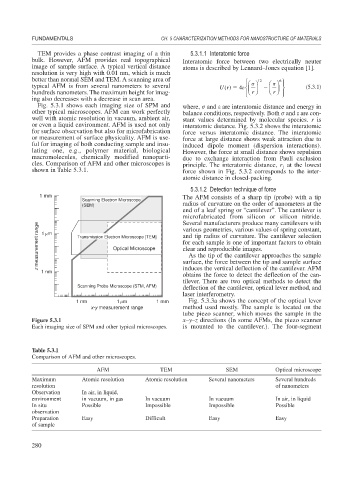
Fig. 5.3.1 shows each imaging size of SPM and where,
and are interatomic distance and energy in
other typical microscopes. AFM can work perfectly balance conditions, respectively. Both
and are con-
well with atomic resolution in vacuum, ambient air, stant values determined by molecular species. r is
or even a liquid environment. AFM is used not only interatomic distance. Fig. 5.3.2 shows the interatomic
for surface observation but also for microfabrication force versus interatomic distance. The interatomic
or measurement of surface physicality. AFM is use- force at large distance shows weak attraction due to
ful for imaging of both conducting sample and insu- induced dipole moment (dispersion interactions).
lating one, e.g., polymer material, biological However, the force at small distance shows repulsion
macromolecules, chemically modified nanoparti- due to exchange interaction from Pauli exclusion
cles. Comparison of AFM and other microscopes is principle. The interatomic distance, r at the lowest
1
shown in Table 5.3.1. force shown in Fig. 5.3.2 corresponds to the inter-
atomic distance in closed-packing.
5.3.1.2 Detection technique of force
1 mm The AFM consists of a sharp tip (probe) with a tip
Scanning Electron Microscope
(SEM) radius of curvature on the order of nanometers at the
end of a leaf spring or “cantilever”. The cantilever is
microfabricated from silicon or silicon nitride.
Several manufacturers produce many cantilevers with
z measurement range 1 m Transmission Electron Microscope [TEM] and tip radius of curvature. The cantilever selection
various geometries, various values of spring constant,
for each sample is one of important factors to obtain
Optical Microscope
clear and reproducible images.
As the tip of the cantilever approaches the sample
induces the vertical deflection of the cantilever. AFM
1 nm surface, the force between the tip and sample surface
obtains the force to detect the deflection of the can-
tilever. There are two optical methods to detect the
Scanning Probe Microscope (STM, AFM) deflection of the cantilever, optical lever method, and
laser interferometry.
1 nm 1 m 1 mm Fig. 5.3.3a shows the concept of the optical lever
x-y measurement range method used mostly. The sample is located on the
tube piezo scanner, which moves the sample in the
Figure 5.3.1 x–y–z directions (In some AFMs, the piezo scanner
Each imaging size of SPM and other typical microscopes. is mounted to the cantilever.). The four-segment
Table 5.3.1
Comparison of AFM and other microscopes.
AFM TEM SEM Optical microscope
Maximum Atomic resolution Atomic resolution Several nanometers Several hundreds
resolution of nanometers
Observation In air, in liquid,
environment in vacuum, in gas In vacuum In vacuum In air, in liquid
In situ Possible Impossible Impossible Possible
observation
Preparation Easy Difficult Easy Easy
of sample
280